Total Pageviews

Showing posts with label Ongoing. Show all posts

Wednesday, June 14, 2017

My Hi-Fi Raspberry Pi DAC project. The Design Phase

    I'm in no way an audiophool audiophile, but I do like to listen to good music coming from a nice bit of quality engineered speaker and amp.
I've had a Sony CD player ( CDP-X303 ES ) for a while now and while it's working nice, it has a huge drawback.
I have to buy a truck load of CDs just so that I can listen to my favorite songs. I tend to have a variety of preferences, mostly based on my mood, that's why I tend to listen to anything from Michael Jackson to  Linkin Park and from Run DMC to Eminem. And anything in between.

     It's much more convenient to download ahem.... BUY my favorite tracks and store them on a drive and listen to them from some kind of network DAC. It's also easy on the mind to know that if a track has some kind of artefacts in it, (Sone CDs I bought have these) you just delete it and downl.... buy another. Unlike CDs, where you just have to live with the thought that something you paid money on  has random shitty, thunderous noises on it. 

PS: Don't buy the Michael Jackson CD albun "The Essential Michael Jackson" from Sony Music. You'll be trully regret it if you do. At least, I did.


A Networked DAC


    So, first of all, I need a board that links whatever DAC I'll make, to my LAN at home, so I can access the songs. And  it'd be nice to also play them.
   It'd be even better if I don't have to spin a whole board for this, so I'm thinking something along the lines of an Arduino or Raspberry Pi.

    I want to be able to play stuff like FLAC or WAV at something like 192 to 380 Kbps, 24 or 32 bits. Also, the few DACs that can handle these bit rates have an I2S (no, it's not a typo) interface, and conveniently enough, a few platforms have an I2S  bus available.
  One such platform is the Raspberry Pi. It's  cheap, has a ton of processing power and best of all, there are a lot of debians and ready-made software for it, covering almost anything you can think of.
  Another option would be the Odroid., which also has enough umph for the task at hand.

  For those cringing at the sound of using platforms like these for Hi-Fi, please keep your composure.  Your finely-tuned ears can't really tell the difference between a 1000 $ DAC and an embedded platform with a good DAC on it (except if the latter is poorly designed). 
  Now, having said this, please excuse me while I go put on my flame suit.

    My decision went in favor of the Raspberry Pi platform just because I happened to have one around.

A quick search for a Raspberry debian that can handle all you music via a network interface will produce the following results:

 - Volumio
 - Rune Audio
 - Etc.

    There are a lot of web players out there that do  the same thing. My personal choice was Volumio. Why did I choose this over the others I hear you ask ? Well, because this was the first result that popped up on Google.

Which one... which..one... Hmm...

    So, having solved the networking part, now all I need is a DAC that can do everything I want i.e. up to 382 Kbps at 32 bits.
A friend of mine did a similar project and he used the PCM5242 from Texas Instruments. It has a very impressive spec sheet, both in performance and in size. But the size is mostly due to its internal DSP. Yep, this DAC also has an  mini DSP inside. Wicked! That opens up a whole new world of opportunities.

Where's the rest of it?

    Anyone looking at the datasheet for this can plainly see the banner on the front page, where it says it has  a DSP inside it. But if you go on further, you start  to see that the datasheet is incomplete. It's missing some of the data on the DSP registers. Bummer. Plus, if you want to program it via an interface, you need TI's Pure Path Studio software...which can not be downloaded from anywhere. You have to send the guys at TI a mail with a request for it.

    Also, take note that there are a few commercial Raspberry shields out there that have the PCM5242. These claim it has a DSP inside  it, which is correct. Unfortunately, if you want to use it or program it, or do anything with it, other than just convert bits to sound, you're on your own. You basically have to create your own library for the PCM's DSP so you configure every bit of it.

    But let's not let this small drawback keep us from implementing what would be a very capable DAC
  I'm going to build one to see how it sounds and how it behaves and if I like it, I'm going to design another version where I try to use the internal DSP and actually put the whole thing to use.

Actually designing stuff

    Ok, so let's see how we're going to do this.
First thing's first: a normal I2S interface uses 4 wires.
 - A master clock, to time the whole thing - MCLK or SCK;
 - A bit-rate clock, BCK, that tells the DAC what bitrate the song is being played at, i.e. you sampling frequency;
 - The data line, DIN
 -  And a signaling line  - LRCK - to tell the DAC which frame of  data is for the right channel and which is for the left one.


Fig.1  I2S Bus with all 4 signals.BCK is derived from the MCK


Fig.2  I2S Bus implementing only 3 signals. MCK is 
internally reconstructed from the BCK

    Normally, the master clock would have to be set so that it is a multiple of the BCK. This means that with most network  DACs (I'm talking about the system as a whole, not the DAC chip itself) you need to have an external clock feeding the DAC directly, or an interface IC, (bridging something like USB - I2S) when an interface conversion is necessary. This is kind of cumbersome and adds a lot of parts to your BOM.
  If you are curious, you can have a look at XMOS's line-up of chips. There are some that go up to 192 k.

    But the PCM5242 only needs one clock - the BCK. It can take this and rebuild the master clock with an internal PLL, thus saving a lot of board space and simplifying the design.

   The 5242 can work either in Hardware mode, or Software mode.
 Hardware mode is kind of a stand-alone thing. You just feed it 1s and 0s from an I2S bus, then it converts them to sound. Easy. You also have some pins with which to control signal attenuation, and that's about it. I'm over-simplifying, but you get the point.

    Software mode is where the magic really happens. You still use the I2S bus, but you can also do soft muting on the DAC, you can control the volume in much finer steps, set PLL frequencies, write internal registers and also, my favorite, control the DSP. All this through an I2C or SPI interface. Your choice. Or, rather my choice, to be exact.

  The prototype is going to just run in HW mode. I don't want to deal with writing any internal registers and doing power ON/OFF sequences and stuff like that. At least, not just yet. I just want to see it work....or to be more precise, to hear it work.


Down to the nitty-gritty


    Ok, so having settled on hooking the DAC so it works in Hardware Mode, what other egineering stuff do we need, to make this thing work?

    My Sony amp has 1 Vpp inputs, but from what I've seen, it can tolerate higher peak-to-peak voltages. Up to 4 or 5 Vpp. I actually scoped a Sony 339ES CD player and got as much as 7Vpp.
 But for safety's sake, let's choose a maximum output voltage of 2 Vpp for the DAC hat.

  The DAC itself can output either 4.2 Vpp or 2.1 Vpp levels. So, let's go with the 2.1 Vpp.
Now, I'm kind of weary about powering the amp's input directly from the DAC, so  I want to put a buffer between them.
 Because I'm lazy,  and don't want to mess around with op-amps possibly oscillating like crazy, I'm going to go with the TPA6120A2 audio amp as the buffer. That's the one in the DAC's data sheet.

  Thus, the final output will have a level of about 4 Vpp (the amp's minimum gain is x2) but we can solve that with some extra attenuation from the DAC. For this, you just implement the table below so that your signal has the needed level.


Analog and digital power supplies design

3.3V PSUs

    The DAC needs both an analog power supply and a digital one, both 3.3V. This isn't such a big deal. But I can sure as hell try and make one out of it.

    One can easily fit a small SMPS or two on a Pi hat. The problem is however the noise these will generate. Ok, this, and the fact that some audiophiles will cringe at hearing the words "SMPS" and "Hi-Fi" in the same sentence.
    I want everything to be as clean as possible, noise wise, so my solution was to split the power supply from the main DAC board. Not only that, I went a step further and split the analog and digital supply, each having its own board.

    Having this configuration however can be more detrimental than helpful. One might be tempted to think that a current's return path would be that of least resistance to ground. And that is correct.. But where that ground is, that can be a bit tricky to find.
  In the set-up I proposed, the ground is not the one on the DAC hat i.e. the PCM's GND connections. It's the one way over on the PSU. So, the actual path would be DAC → about 5 cm of wires (2 inches for the non-MKS lovers) → PSU GND
With such a large loop area,  it's an open invitation to a whole lot of noise pick up, no matter how quiet the actual PSU is.

 I tried to mitigate this by having the PSUs regulate down to 5V for the PCM's power rails then have an additional LDO on the Pi hat itself, to do the rest of the work down to 3.3V. This  (I'm hoping) will "bring back" the GND return path to the hat. The current loop this set-up creates is the shortest possible.

To split o not to split, that is the question

   A recurring issue in this Analog-meets-Digital world appears: how to manage the digital and  analog ground planes for the DAC?
Having both an analog and a digital rail, how exactly do you route the grounds on the board so that you get the lowest possible EMI and the least amount of noise pick-up on you signal lines? Do you split them clear through the middle and place the DAC right on the center line? Or do yo just make on continuous plane?

  There are lots of articles  dealing with this exact issue, and depending on when it was written, you might get some diverging answers.
I have come across a couple of articles that explain the issue very well.
One is this article, which kind of gets you on the right path. If you need to go deeper down the rabbit hole, I recommend reading "Grounding in mixed-signal systems demystified", parts 1 and 2, from Texas Instruments.

  Following the general direction from these articles, I decided to only join my grounds under (or close to) the PCM DAC and exercise the right routing technique so that I have no analog signal wires crossing the digital ground or vice versa.
  Now, for this design, it's pretty easy to get things right, it's only going to be a two layer board and there are only 4 ICs and some passives on it, but for other designs, it can get messy when routing signal lines across the PCB, and keeping  the traces in their right ground plane can cause you some head aches

Cap selection


  No, I don't mean electrolytics. That's a discussion for another time.  I mean SMD ceramic caps. As in MLCC caps.


In this design, there are a few places where caps really matter, despite being used mostly for bypassing.

    The 3.3V regulators on the DAC board are LP2992 LDOs. Yes, Texas Instruments again. Now, these are advertised as having very low noise, and to achieve this, the datasheet recommends using some very low ESR caps on the input and output  and NP0 or C0G caps on the Bypass pin.
   My personal choice was to go with X7R caps for the 5V input and 3.3V output caps. The rest of the bulk capacitance will be on the PSU boards.
These have much lower ESR than electrolytics and behave much better under DC bias than X5R caps. Tantalums are on my naughty list and try to avoid them as much as possible. They don't take voltage spikes that well and their ESR isn't really that low.
    Also, the X7R material is less sensitive to changes in capacitance due to temperature and/or DC voltage (compared to X5R, that is).

  NP0 and C0G dielectrics are literally in a higher class than X7R / X5R. While one might use the latter in normal bypassing applications, the NP0/C0G can be used in filters, or for setting precise time constants. If you were to plot a frequency vs capacitance chart, you'd get pretty much a straight line from DC to about 10 MHz and a somewhat linear temperature coefficient.
This makes them very useful for, say.... some nice RC filters that go on the output of a DAC. And it just so happens that we have some of these between the DAC's differential output and the op-amp's input.

  You can find a lot of info about this on the net, so I won't bore you with too many details. You can check out this document I found in haste, while deciding which type of cap I should use. It's got graphs and tables in it , so it must be good.


Hardware Mode configuration pins


  Like I mentioned earlier, the PCM5242 can be used in Hardware Mode or in Software Mode, making it a very flexible design.


  First off, to put the DAC in Hardware mode, pins 24 and 23 need to be pulled low.
Now, there aren't many control options left. You can choose between a 2VRMS output or a 1VRMS output by making pin 21 Low or High, respectively (i.e. 1V out for AGNS high).

  I've already talked about the attenuation output pins so that's the important bits taken care of.
What's left is to set pin 16 Low, because we don't want any de-emphasis, and if you don't want to hear any hissing in your speakers when nothing's playing, then you'd want to set pin 1 Low.
There, that about covers it.


Schematic and PCB Layout

    If you're interested in building something similar or just want to have a look over the schematic, you can go to my GitHub  project page. There I have all the documents relating to this project. Feel free to download and/or use the desing as you might see fit.

  The laying out of the PCB went pretty much as I'd expect it for this simple design. Like I wrote, I opted to do the joined AGND and DGND sollution.
Unfortunately, because I wanted the bypass caps for the DAC as close to the pins as possible, I didn't have ena clear way to split the ground right beneath the DAC, so they're joined in two locations, either side of the DAC


     This may look weird, but I don't think it impacts the noise performance of this thing too much. But, if you believe otherwise and have more experience than me, then please leave a comment below, I'd really like to hear some nice explanations.


    So, basically, this is what I'm expecting to get from the PCB manufacturer. Except in black. It's going to be gorgeous.
Oh, and for those of you wondering what those holes on the bottom of the picture are.... wel,, I figured I'll just solder the audio output cable straight to the PCB. And to firmly hold the cable there and not put pressure on the solder joints, I figured I'd zip tie the cable to the PCB. A bit flakey? Maybe. But I  didn't want too many metal to metal interface between the output of the DAC and the input of my speaker amp. I may possibly be dellusional here, but hey... I like to experiment.

  The PSU layout also went snoothly and looking back, I could have squeezed both PSUs onto a single board or two smaller boards than the ones that came out. Next time I'll know better.


    Now, all that's left is to wait for the boards and parts to arrive.

  If you would like  to read on about how I put everything together, tested this and how it all turned out, the second part of this build is here.


Disclaimer: The stuff from TI I bought myself. I'm in no way affiliated with them. It just happened that they have the kind of parts I  needed


Tuesday, April 4, 2017

Transformer Coil Winding Jig

   
     If you can do it, then why not over-do it. At least that's what I did with this project. It started out small....just a simple motor, stick a bobbin on the end of it then wind away to you heart's content....Naaaa!

I need to control this...

Indeed, I do. And since  this will be a "hand winding" operation, it implies that both hands will be preoccupied with the....well, winding, of course. Therefore, who's going to control the motor? 
And since humans happen to have four limbs, an obvious candidate to fill in the position would be - a foot...by means of a pedal. Ergo, I need to make myself a foot pedal to properly control the motor. And not just an ON/OFF kind of control. No no no....I want speed control.


Choices... so many choices....


    Ok, so how about the heart of this thing? The motor. What kind of motor should I use? Well, a DC motor from an electric drill would have been enough. But like I said, why not overdo it. So, I had a Stepper motor driver available. It's an AMIS-30543 stepper motor driver that can do up to 3A per coil. Works for me.


   Now what kind of stepper? Some might think, "a NEMA17 stepper would do it". Not! 
From my pile of steppers, of course I went ans picked the biggest  most powerful stepper I had. It's a NEMA23, 3Nm  stepper motor. You might think it's overkill. But Since I do a lot of SMPS and high power stuff, there will come a time when some 0.7mm or 1mm magnet wire will have to be wound. And that requires a lot of torque at low speed. Yes, an electric drill ca provide that. I know, I know. I just don't want to use that.


Strange things are afoot


    Now for the control part - The pedal.
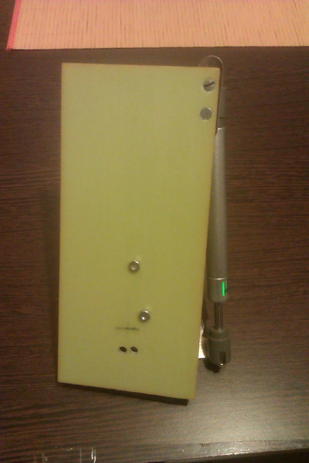
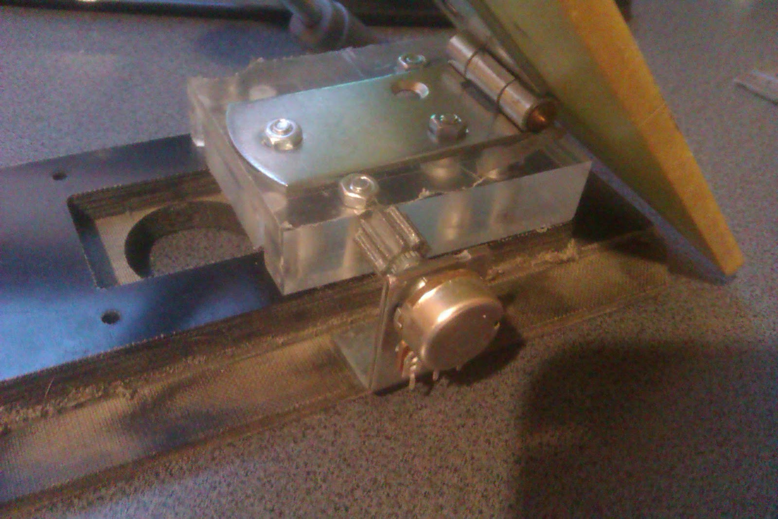
I initially though I could do the pedal with springs... big powerful springs. Of course, that didn't really pan out. The spring itself was OK, but the wire setup would either get snagged or the wire (guitar string wire) would stretch out and  wouldn't tension the spring properly.
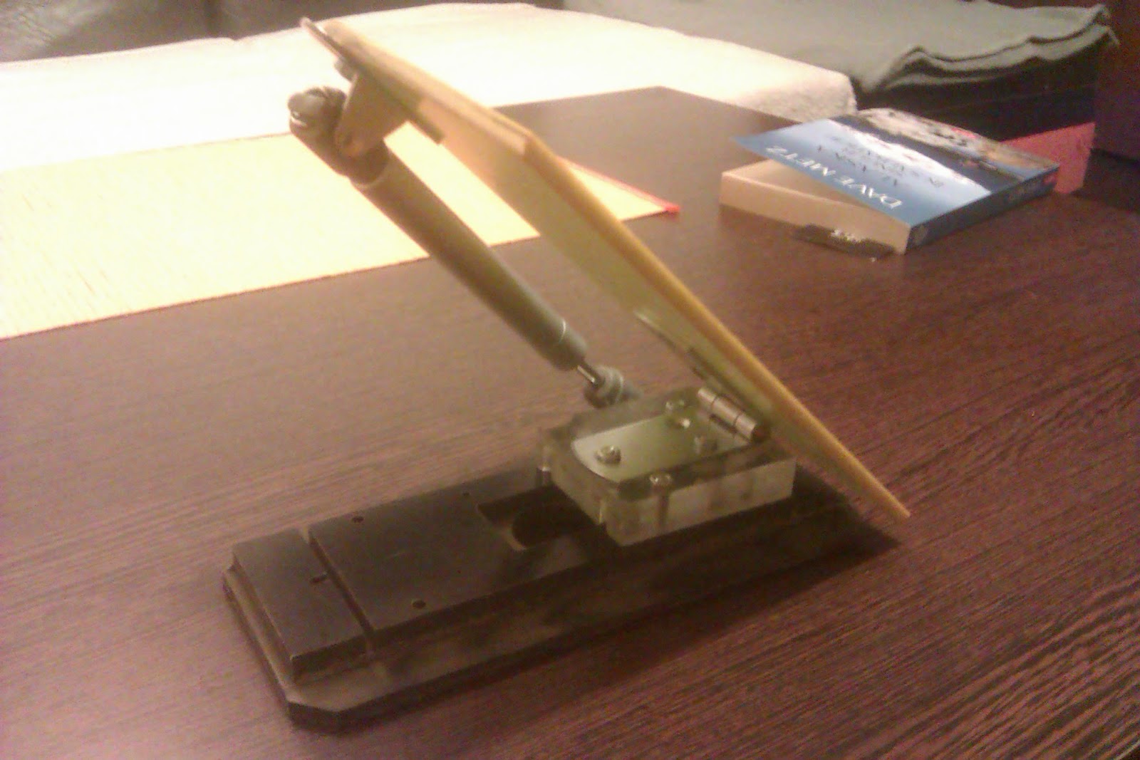
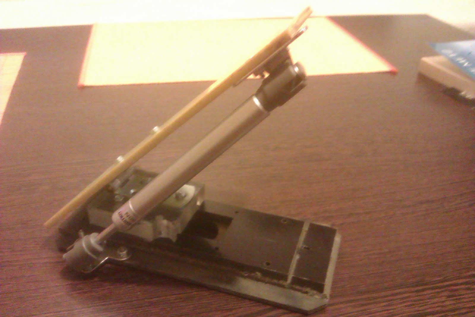
    But, being the engineer that I am, I often get inspiration from things around me. This time, it was a cupboard door hinge that used a telescope to help raise and lower the door. BINGO!

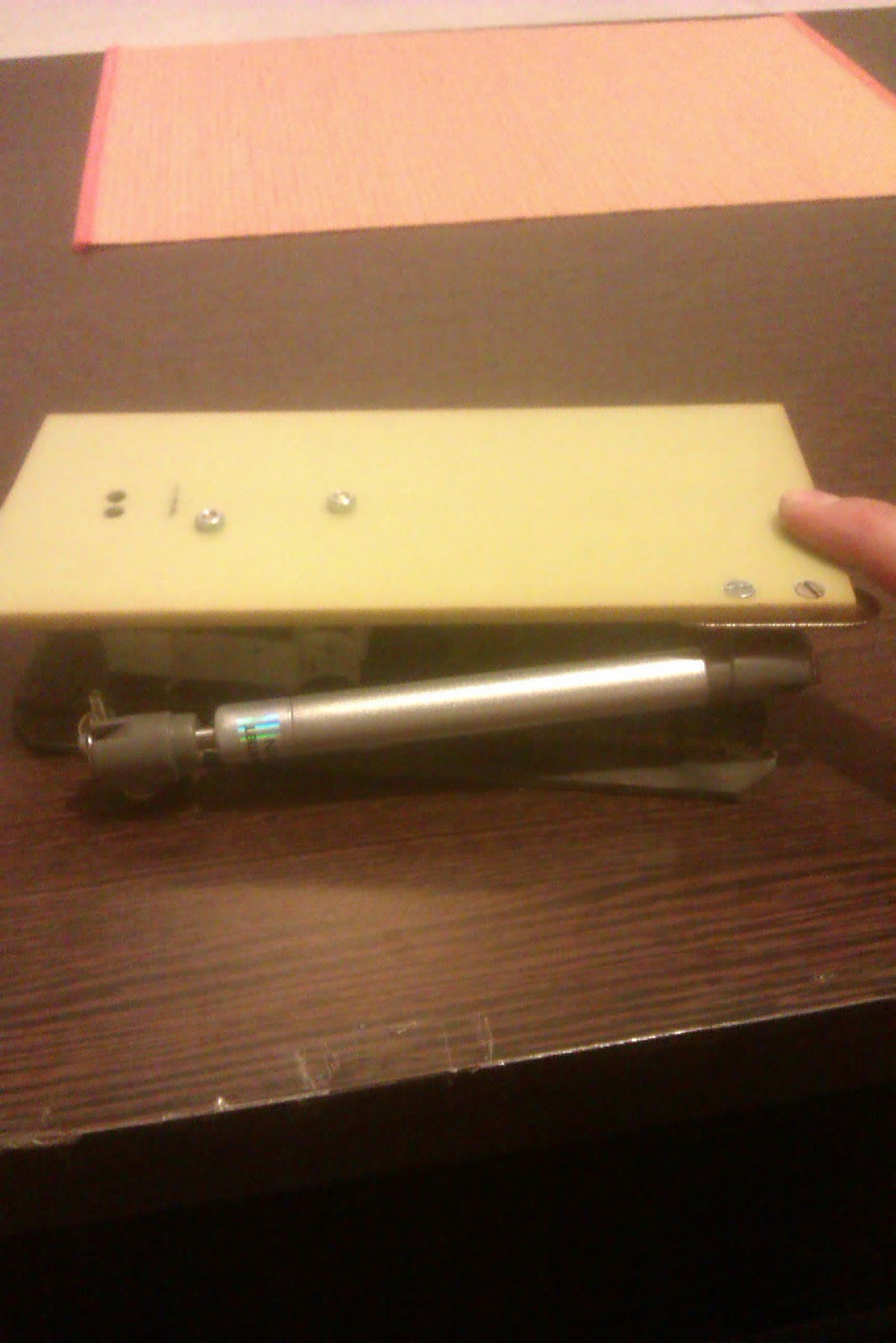
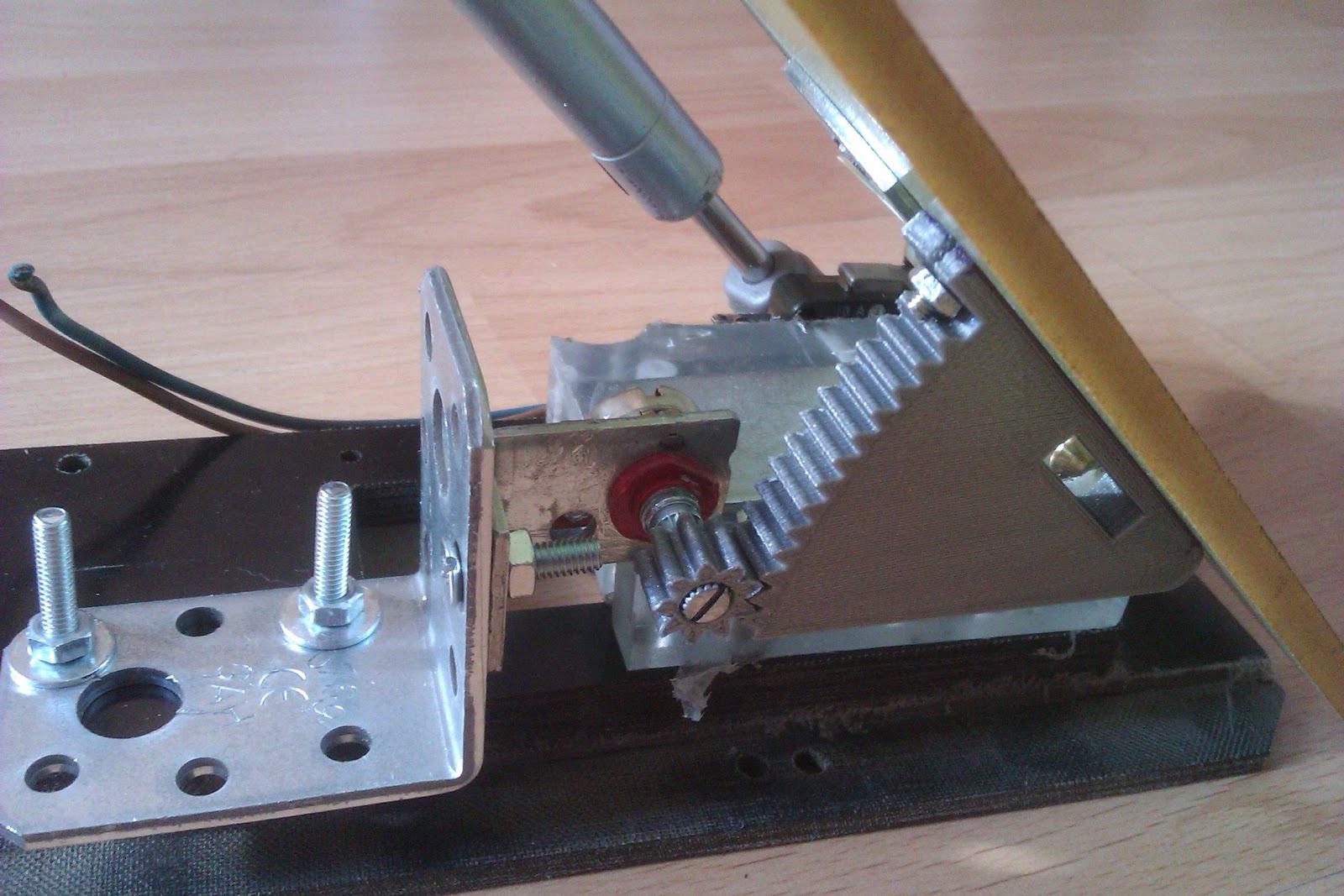
I went to the hardware store, bought two of those furniture telescope things, came home, threw away the spring and wire and mounted the new mechanism. And it worked. Brilliantly, I might add. It feels just right. The pressure i have to put on the piston feels just about right. And it's very smooth and controllable.


The two nuts sticking out  in the middle of the pedal will eventually get replaced by countersunk screw...eventually.

The base is made out of  15mm (590 thou, for those that still refuse to get with the program) thick resin impregnated fibres (cotton fibres, I think). Atop of that is a square polycarbonate piece, that holds the hinge. The pedal itself is made out of some kind of  5mm thick fibre-glass resin material.

If you're wondering about the routed edges and other stiff going on on the bottom black piece, well, don't They were already there. (I'm not that lucky as to posess a milling machine....yet)

Now, I mentioned earlyer that I also want to have speed control.
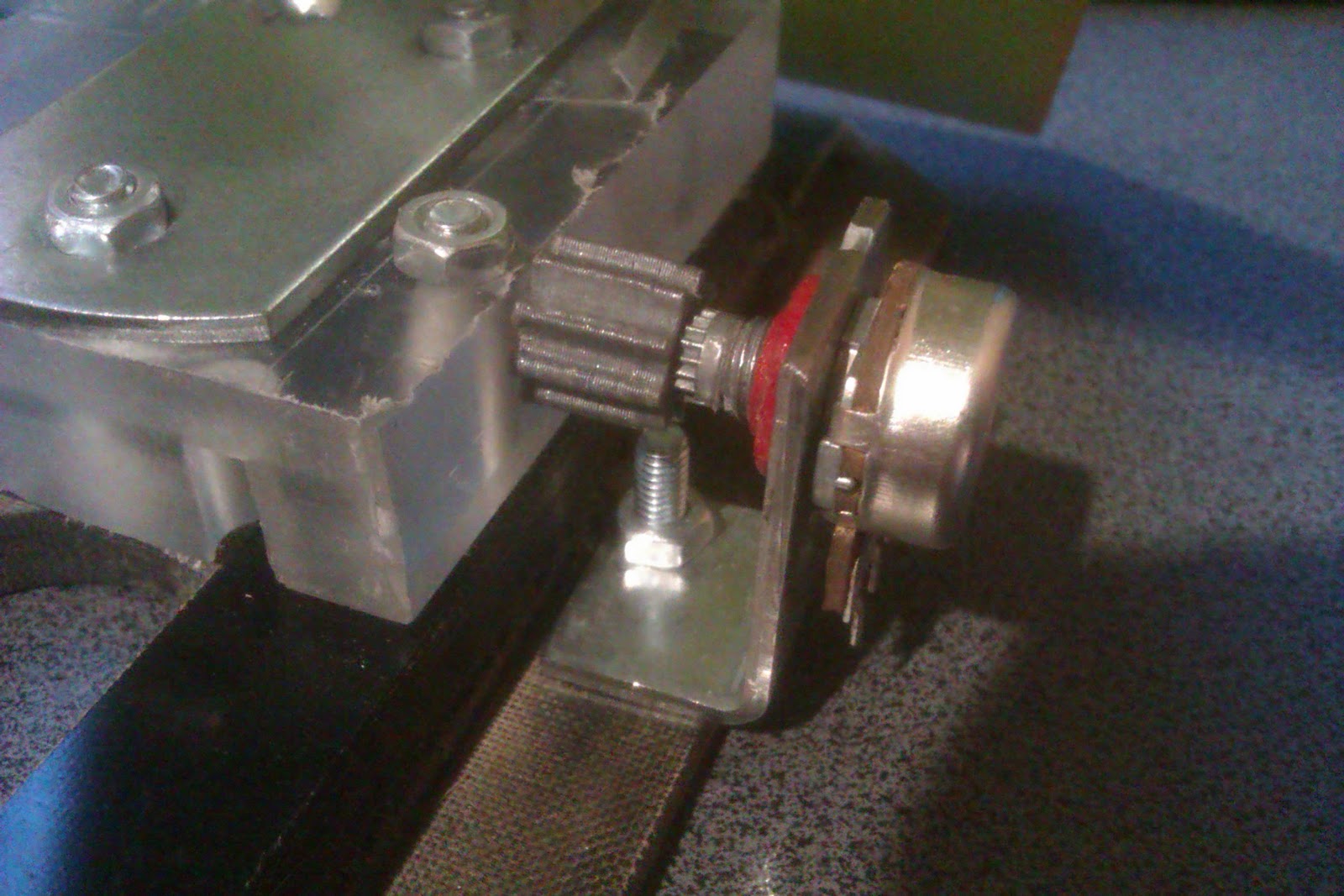
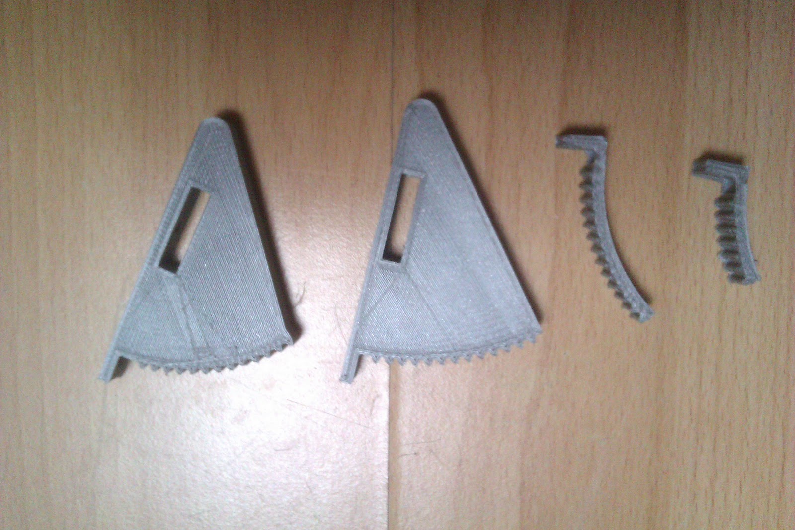
That is done with a regular 10K potentiometer and a rack and pinion set.


The parts were designed and printed by yours truly. Ok, only designed.. my 3D printer took care of the actual printing part.
 The travel of the pedal actually matches to the 3-quarter-turns of the potentiometer. If you want to know how I did that....luck. Pure, dumb luck.
I thought I'd have to do some iterations before I got things to properly mesh (radius of the rack, number of teeth, pedal travel) but somehow I got it all in one go....


Or maybe not...


Keeping count of things

120...121...122...130... Obviously, it's not an improvement to hand winding if there isn't a way to keep track of your turns.
That shouldn't be too hard. The whole jig is already controlled by an Arduino, and it still has a lot of free pins. So let's use them.
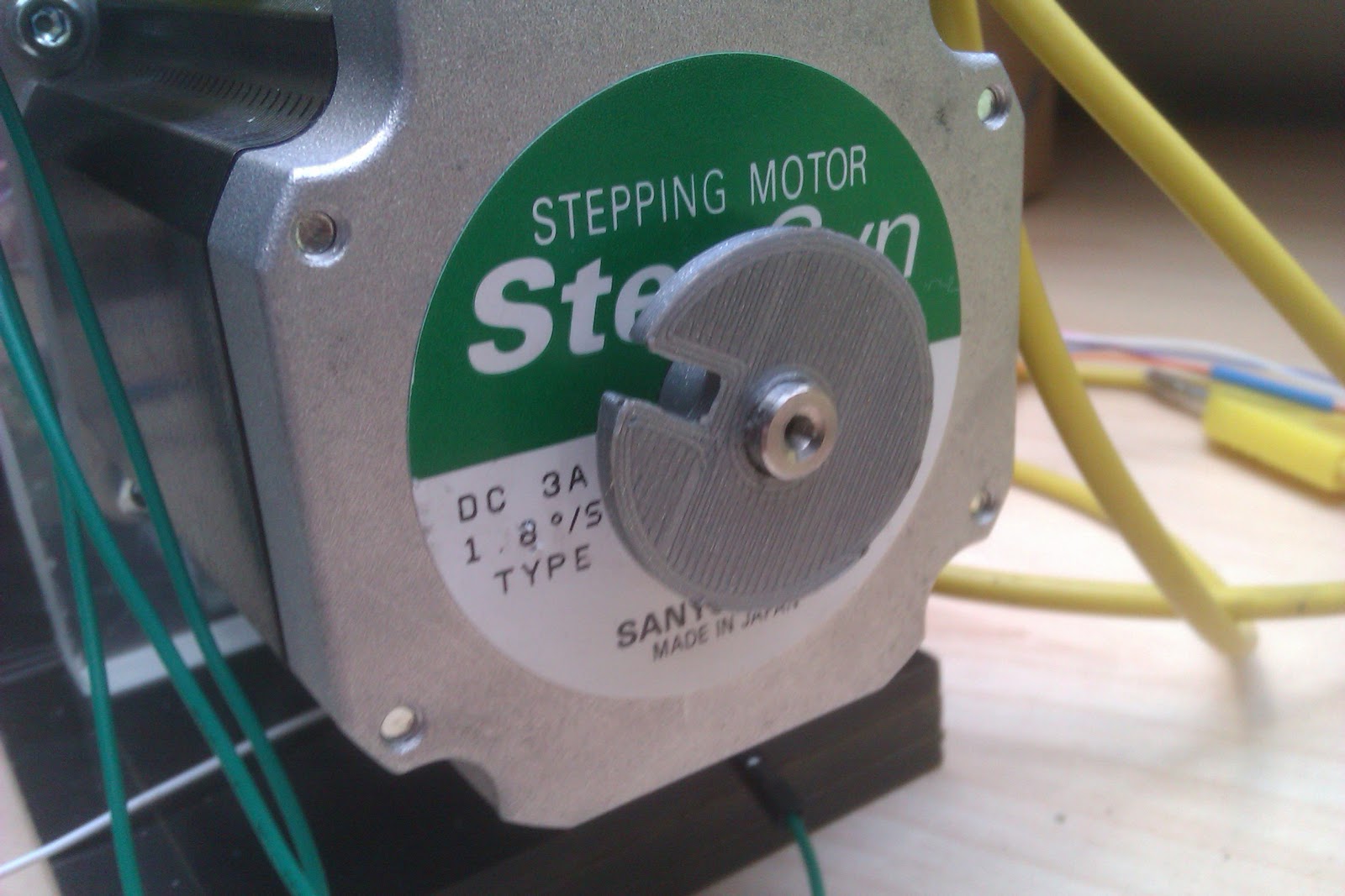
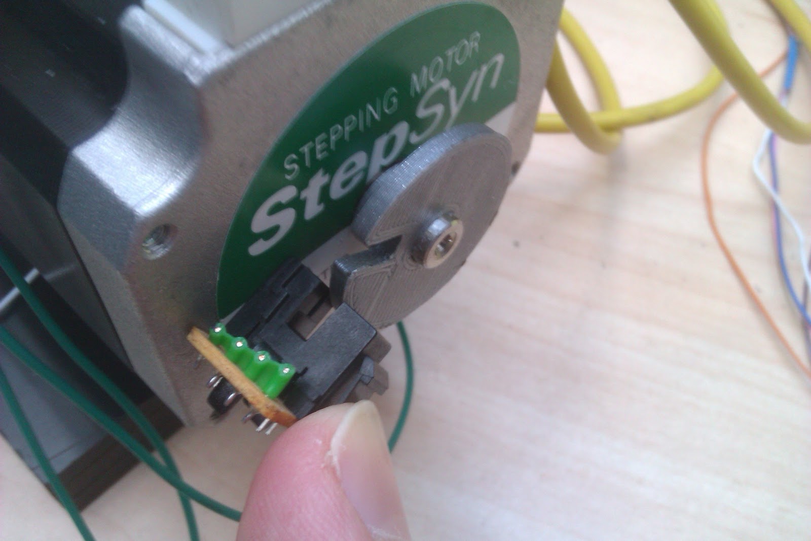
   And since the motor happens to have an extended shaft out the back side, why not stick an infrared light barrier and a small wheel with a slot in it, on the shaft?
 When the motor makes a full turn, it lets some light pass, the Arduino increments a counter on a display....Perfect!


The wheel was 3D printed and you can find the STL and Solidworks files for it right here.


Putting all of it together

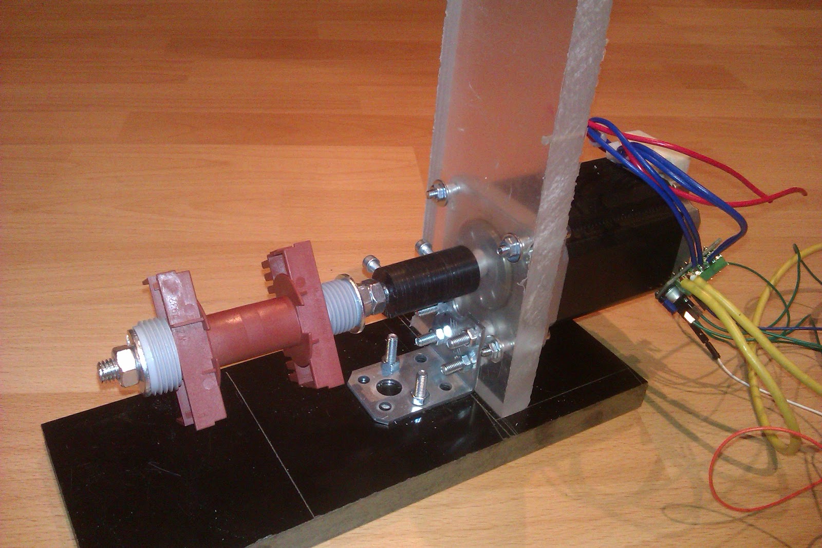
I had to build some kind of stand, for the motor. Once again I used some 15mm black resin impregnated fibre material  and some 15mm thick polycarbonate scraps that I had.

The stepper was bolted to the frame with M4 screws.


It may not look like much, but the whole frame, once everything was tightened down is verry sturdy and can take quite a beating from that stepper.

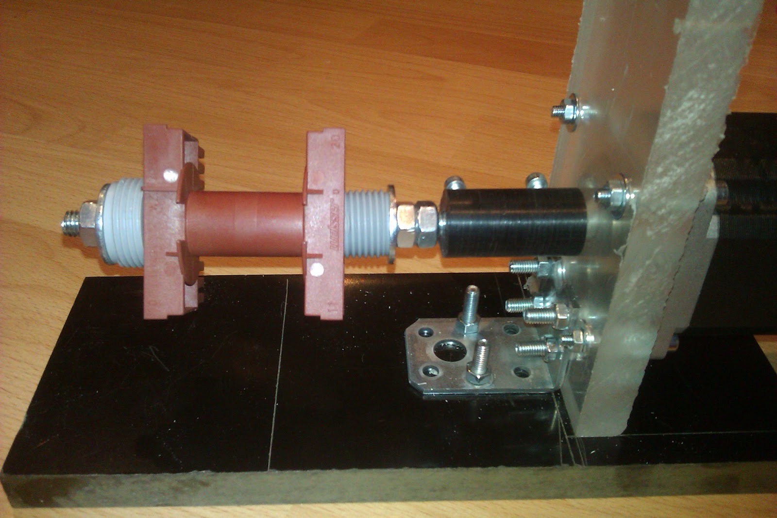
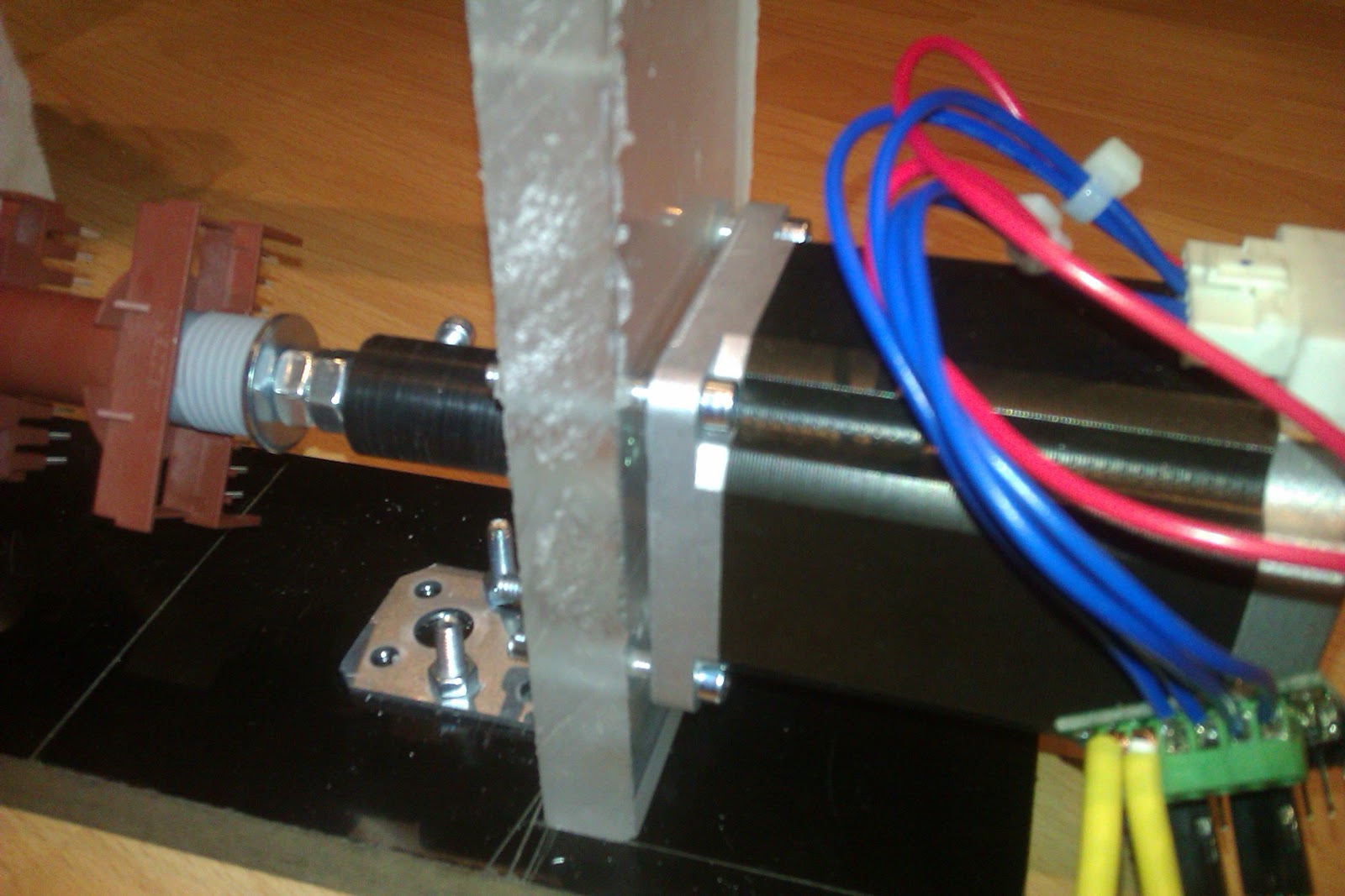
The black cylindrical thing is a home-made shaft coupler. I had some black delrin around that I bore on either side, to allow the 6.35 mm stepper shaft to couple to some M8 threaded rod. To keep the shafts from turning inside the coupler, I drilled  two 6mm holes in the side of the shaft coupler then put in some brass inserts. Two M4 screws go into the inserts, locking the shafts to the coupler.

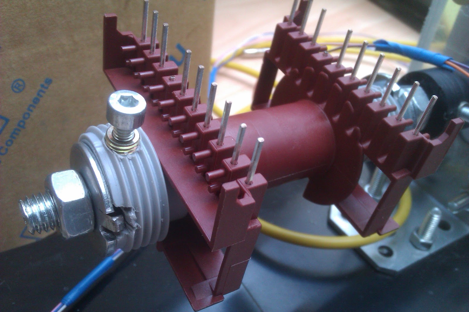
On the threaded rod I put some nuts as spacers and some Gardena hose adapters of some sort (the grey plastic things), that just happened to be the right shape to keep the ETD49 bobbin in place.


 I've also cut a slot in each of the grey plastic retainers and filed a mating pertrusion in the metal washers so that they wouldn't slip and turn ith the main stepper shaft. Of course, the plastic thingys will eventually be replaced with some proper 3D printed retainers, but who knows when that will be.


Sharing is caring

All the files for this build can be found on my GitHub page. These include the code for the Arduino, the SolidWorks and STL files for the optical rotary thingy and whatever else I may find useful to throw in there.
As always, you can enjoy the full splendor of crappy quality pictures of the build here.


Friday, November 4, 2016

TwinTeeth Plus Build Log - Part 1


I want a PCB and I want it NOW!

      Have you ever had a burning need to design, layout then etch a 2 sided prototype PCB, at home, before you send it out to a PCB fab, to make sure everything is OK?
Well, so have I.

      I came across a PCB "design bundle" that I really want to try out and  build. 
This will be  the first in a line of blog entries, detailing my build process and review of this. 
Because of it's open source nature (nice one guys, thanks!) I had everything I needed to modify and adapt my design to fit the parts that I had. 
Therefore, along with these posts I will also upload the files for the parts that I redid, just in case someone happens to have some of the parts that I had.

...but first, some background on this

      I've spent a few weeks looking around for ideas on how to PROPERLY make a device that moves on 2 or 3 axes and  has a UV laser for a head. I wanted this to do a line-scan on a UV resin-coated PCB board, then etch it and have a prototype PCB done in  a matter of 30-60 minutes.
I quickly came to the conclusion that a  traditional gantry-style  CNC machine wouldn't cut it, in terms of speed.

      So, thinking about other stuff that has a scanning laser, I thought about how fast laser printers work. Then I began looking at trying to control a mirror array from an actual laser printer. 
In theory, it wouldn't be hard at all. Just have a hexagonal mirror spin on a spindle, shine a UV laser on it then pulse the laser so it will scan the board one line at a time. But, as always, the devil is in the details. 


      Suppose you have a PCB that's 10cm x 10cm. The laser position is fixed. All you're doing is generating a scanning pattern with the hexagonal mirror. That means, that relative to the center point of the PCB,  the laser beam will have to travel 5 cm in each direction (5 to the left and 5 to the right). This means that the beam length will be altered by ± 5 cm. 
According to physics, if the length of the beam changes, that means that the focusing of the beam will change also. 
What that means is, with a fixed focus, as would be the case in a scanning head, the beam will be focused in the middle of the board and it will be slightly out of focus on the edges of the board. If you have a laser beam that is not properly focused, it will leave behind an image that is blurry. 
And if you're doing  a board with, say, 0603 components on it, the pads will come out looking more like blobs of copper.

      Of course, laser printers have the same issue. The way THEY solve this is  they have  an  f-Theta lens in the beam path.
      For those of us that don't have Stephen Hawking  on speed-dial, an "f-Theta" lens  will take the incoming FOCUSED  beam of light and keep it focused, no matter the angle it's outputted at (or, put it another way, along the scanning path,  the beam, it will be focused in any point)

                                        Source: http://www.opli.net/opli_magazine/eo/2014/optotune-demonstrates-new-laser-processing-lens-aug-news/

...Houston, we have a Problem!

      So, let's just Google "UV f-theta" lens and see what we'v....OH MY GOD!!!  How much?? F*** it! I'm taking up ballet lessons.

So, after I drank a cup of water, took a few Xanax pills and did that "Wax on wax off" move, I decided that I had to go back to the initial gantry style of CNC machine.

Note: for those curious enough to ask, a laser printer uses a RED laser. The PLASTIC f-Theta lens in a laser printer is NOT suited at all for the UV laser. The plastic the lens is made of  is not transparent to UV light.

...Long story short....

    So, eventually,  after searching the net for all kinds of ways to solve this, I found this site: http://www.diyouware.com/DiyoPCB-MKI and my jaw just dropped. Now, how about that... that was EXACTLY what I wanted to build.

But first thing's first: let me congratulate the guys (and gals?) over at Diyouware.com for their hard work. Hope to see you in a Kickstarter campaign soon enough.
And no, I'm not in any way affiliated with them nor am I getting any money from them for writing this.
So, with the disclaimers out of the way, on with the story...
     I  began reading what these fellows did and how they hacked the Blu-ray laser head of the Toshiba drive. Of course, I contacted d the guys, and they recommended me the TwinTeeth variant of the PCB factory. The reason was that the original Mk1 design was kind of clunky and plagued with problems generated by vibrations.

Let's get building

      Now, I have to say, I really appreciate what these guys have done. They did everything from scratch, even developing their own hardware and software platform. 
And they've open sourced everything as well. To me, this is awesome, as everyone can get the files and make their own build, modifying it where possible and putting their own spin on things. So guys, a big  thumbs up from me!

I've decided on building the TwinTeeth Plus version, as this has less 3D printed parts and to me, looks to be more stable mechanical wise.

First off, I got me some 2 mm thick aluminium sheet (I couldn't find any 3mm plate)


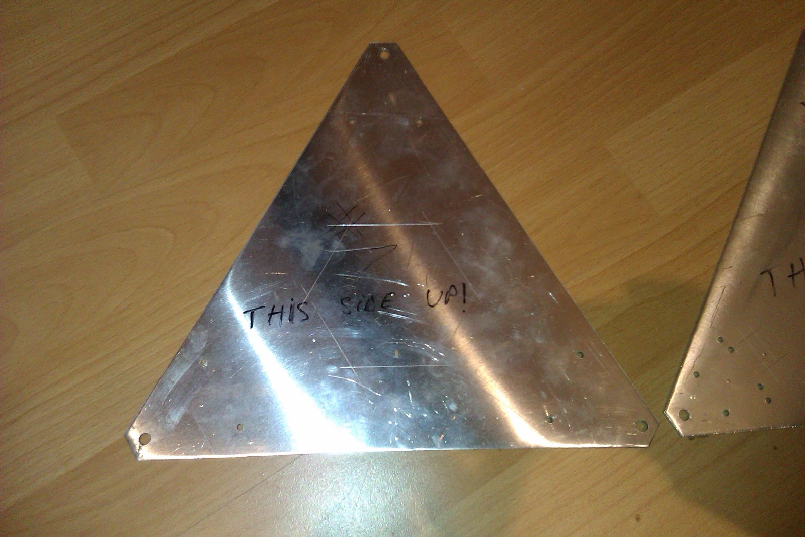
On these, I glued (OK, scotch taped) the paper templates then marked where the holes would go.

After this, I went to print the 3 motor holders that the delta sits on. And here is where the real fun begins...
Looking through my collection of stepper motors, I happened to find 3 identical NEMA23 steppers. 

 The original TwinTeeth  needed NEMA17....Yes, this is one of the advantages of having a mechanical engineer for a girlfriend (Thank you!) She helped me modify the motor holder .STL file, so that it took the NEMA23 motors.


Next up were the bottom lead screw supports. Some F6900ZZ flanged bearings were supposed to be fitted into them. 
Because these bearings seemed to proliferate in the wild planes of eBay, but nowhere near my country and because I got burned by the national postal service (which sucks) too many times,I decided I would replace the flanged bearings for "normal" ones. (flanged bearing was d=10 mm, D=22 mm, 6 mm width; replacement bearing is d=10 mm, D=26 mm, 8 mm width)
 This meant firing up Solidworks and doing my magic. (I was stubborn enough that I wanted to do the part from scratch, by myself - what better way of learning Solidworks)


Unfortunately, the original dimensions in the .STL files have some wacky values, which proved to be a real pain to replicate. I had to build my own geometry on top of the .STL par to get the dimensions I needed. Then replicated and adapted that so  a 6000ZZ series bearing would fit.

Next, I got hold of some 20mm x 20mm square aluminium profile for the legs, 3x10mm, 200mm long  ACME (AKA trapezoidal) screws which I ordered to be milled on one end to 8mm, so it would fit in a 6.35mm x 8mm flexible coupling and  6 x 6mm, 300mm long guide rails, which I ordered to have M4 bolt holes drilled and tapped into them, at each end.


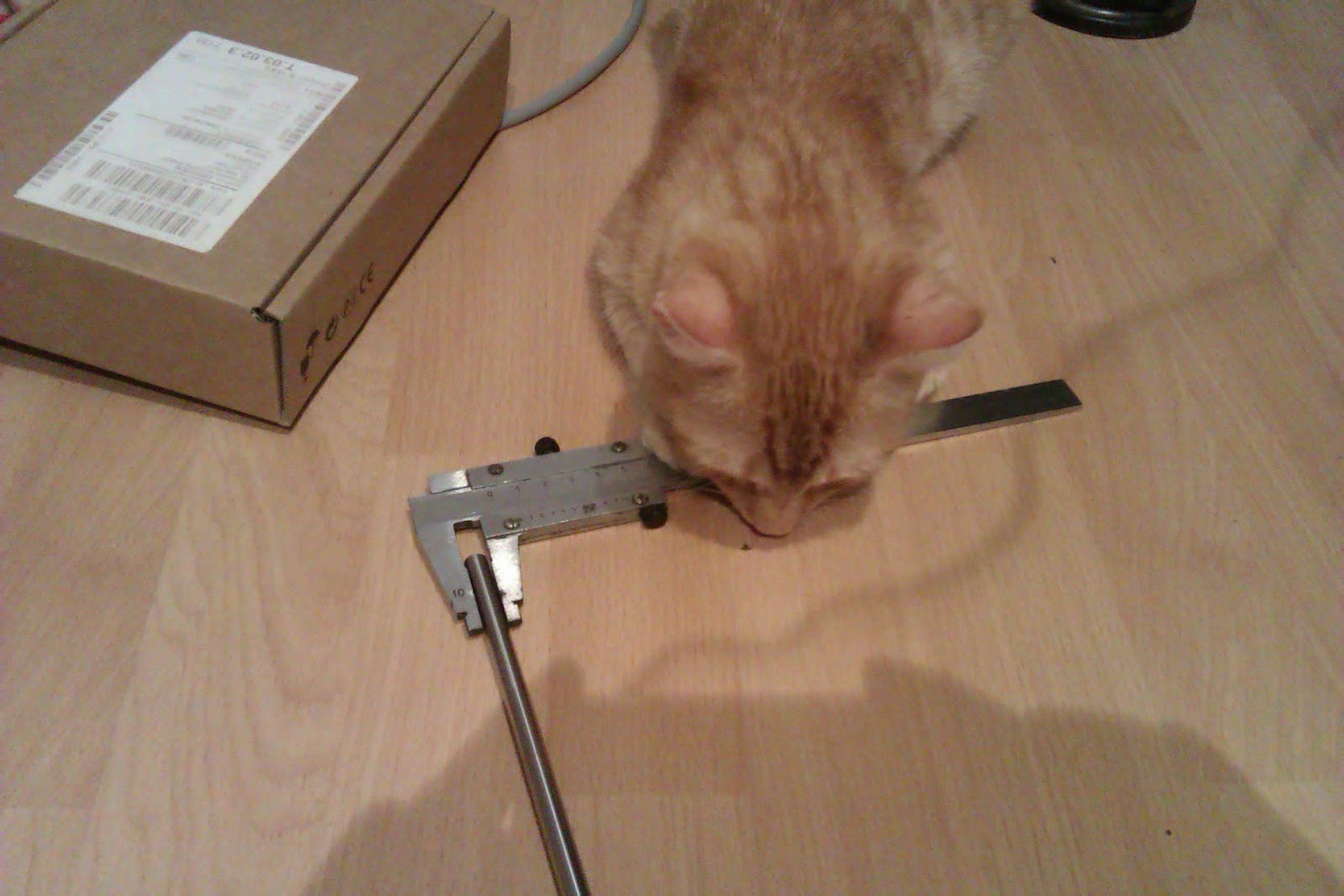
I also got some extra help for this build


He knows the vernier scale can be tough to read sometimes, so any help is welcomed.

Also, I know, the picture quality is really crappy.... I gotta get me one of those newfangled things called a camera. Tin-type photos, anyone?

Inches, millimeters, mills, centimeters....

      The only thing I found difficult about this project so far is modifying the existing parts. It's not that they're in .STL format.... it's the fact that the dimensions are kind of all over the shop.
At least, this is what I gather from measuring the provided .DWG files and the original .STL models. I mean, there are hardly any measurements that seem to have nice round values. I don't know if this is due to the fact that the design was done in inches, then converted to mm, or something else is going on, but it makes things kind of hard when it comes to taking measurements.

...come one, come all....

       This is the link to the GitHub page that contains the modified files. Like I said, I used NEMA23 steppers and  6000ZZ bearings and some of the 3D prints were modified for  MY specific build.
  As the build will continue, I will modify other parts as well. Why? Because it's interesting and because I have  an OCD about improving stuff.
Next will probably be the ACME nut for the 10 mm screws. I don't know if  a bough ACME nut will have more or less backlash than the original TwinTeeth method, where a mold of the screw was made and used as a nut, but those linear bearings held to the mount with  zip-ties...kinda make my skin crawl. 


Tuesday, October 27, 2015

High Voltage Differential Probe Design and Build - Part 1


This project will be made of multiple parts. First, I'll explain the basics of designing a differential probe then the following posts will be about how to actually do the math and lay out the PCB for something like this.
But first thing's first:

"Excuse me, how much is this?"

Have you ever  wondered why are differential oscilloscope probes so expensive? Well, I have, and the answer is....out there?!
No, seriously, I would accept a price of 100 to 150 Euros for a probe, maybe even 200 Euros, but anything over this seems like  a waste of money, considering what these devices have inside them (we'll get into this a bit later). Also, some manufacturers just re-brand  probes as their own and add an extra 50-100 Euros just because it has some fancy well known T.E. manufacturer logo on it.
Lately, the prices on eBay have jumped to some ludicrous amounts just because the sellers think they have the market cornered. Of course. they're just being stupid.

So, WHAT are these things made of?

 For starters, an input attenuation stage which is nothing more than a compensated resistive divider (one divider for the positive and negative input) followed by a differential amplifier. Simple, right?. The input attenuation stage is designed either with two high voltage resistors and two caps in parallel, or multiple lower voltage rated resistors.
After the input signal has been divided down to a reasonable level, a differential stage comes next. This rejects the common mode noise and does some amplification, if needed, then this passes it on to the next stage, where differential to single-ended conversion takes place.
This will be the actual signal that your oscilloscope sees. Follow this by an optional  output stage, if you need that 50 Ohms matching impedance, and that's all.

It may sound complicated, but there's really nothing to it. You could build one for 30 or 40 Euros, designed either for high voltage (1KV to 2KV) and low bandwidth (about 20 MHz) or lower voltage but higher bandwidth (up to 1GHz). For the latter, the design shown here : https://xellers.wordpress.com/electronics/1ghz-active-differential-probe/ is relatively simple, inexpensive and very useful. It'll go up to 1Ghz bandwidth and -20dB attenuation which is all most people ever need in their prjects.

I wanted, as an exercise, to design and build a high voltage probe, capable of taking in a differential signal of up to 1.5 KV and with a bandwidth of somewhere around 15-20 MHz. Also it must have variable attenuation (1/10 and 1/100 or 1/50 and 1/500) and be powered from a 9 Volt battery - this last part is to make sure there isn't going to be any ground loops that can ruin your day and also it makes shielding the whole circuit much easier. Most importantly, it should cost below 50 Euros in parts (does not include the PCB, if I decided to have one made and not go DIY on this).

For starters, I took an already existing design  then replicate that so to keep the costs down.  K.I.S.S. right?
I searched for a schematic (easier said than done) of an existing commercial  differential probe then took that as a scaffolding for my design.
      I managed to track down a schematic on this site: http://www.diyaudio.com/forums/equipment-tools/248505-differential-probe-reverese-engineered.html  which together with with the teardown pictures from here, gave me a pretty good idea of how to go about building the probe.

For anyone trying to do the same, or just and make sense of the schematics from the above link, some values for components are not the right ones. I got some values by cross-referencing the schematic to the actual photos of the probe. What values I could't find at all, I calculated them or mucked around in LT Spice until I got a satisfactory response from the circuit.
This is my first project where I'm working with frequencies above 1 MHz, so bare with me here.


"So I want to build a High Voltage differential probe. Ho do I do this?"

    This is where the real magic happens. Once I had the general idea behind these probes, I got down to the nitty-gritty. Although the input stage is the first one an input signal sees, I started off with the differential amplifier.
The schematics in the previous links don't make much sense, so let me put things into perspective:

                                 Please see the later edit below for an update for this schematic

    Looks friendlier now, doesn't it? Now let's see how this thing works. It's basically just a JFET differential amplifier with some bits stuck to it to make the thing behave better from DC all the way to  a couple of MHz. The guts of this thing is the matched JFET pair Q4A and Q4B. For  those who are just getting to grips with electronics, matched means that both of these transistors are housed in the same package so as the noise and temperature affects them in the same manner and you don't get an imbalance in the amplifier.

    "So, why don't I just stick the output from the input attenuation stage into an op-am  instead of reading this long post? "
Well, I'm glad you asked. Thing is, you want a very high impedance at the input of this probe. Sure, you might have a few resistors of a couple of MegaOhms on the input, isn't that enough? Nope, The more the better. But the bigger the input impedance, the bigger the gain-setting resistors will have to be. And those values, together of the capacitance of the input of your op-amp will make a low pass filter which will slow down the op-amp itself. And when you want to go into the 10-20 MHz region, that just won't cut it.

    "Then, how about we buffer the input with a few more op-amps?"
Yes...and No. You could, but you'd need some high speed op-amps, to form an "instrumentation amplifier" design:

https://xellers.files.wordpress.com/2014/03/simple-differential-amplifier.png 
    But high speed op-amps are expensive. Also you don't just stick the output of an op-amp into the input of another at high frequencies, because they tend to oscillate and do all kinds of other unpleasant things. 
OK, if you actually go and try this with three op-amps that have a bandwidth of, say, 200 to 500 MHz (I'm talking about the Gain-Bandwidth Product here), odds are it will do the business. 

    But there is another factor to take into consideration. Common Mode Rejection. Remember that you'll be measuring differential voltages with this probe. Meaning, you can stick the negative terminal of the probe anywhere in the circuit and measure THAT relative to the Positive one. But that Negative terminal can sometimes be at a potential that is not Ground. It can be at a potential of +150 Volts and the Positive at +300 Volts. So you'll be measuring +150 Volts, but that signal will be piggy-backing on top of another 150 volts from ground, which your probe will have to ignore. 
How does it do that? With a high Common Mode Rejection Ratio (CMRR).
The three op-amps previously talked about will most likely work, but the  low CMRR of the design will let you only measure voltages that are near Ground potential. (a few tens of volts, maybe a hundred or two, depends on your choice of op-amp). Most op-amps tend to have a CMRR that drops the further up in frequency and gain you go.

    Sorry for the long detour, but this was needed to explain the whole idea why a JFET differential input should be used (at least in my case).
Now back to the story. 

    "So, we're going to be using the JFETs. What do the rest of the things in the circuit ACTUALLY do?"
   Another fine question. So, starting from the top, R13 and R24 are drain resistors that set the gain of our differential stage. The gain will be G = gm*RD where gm is the transconductance of the JFETs and RD is the value of R13 = R24 (the drain resistors).
Now, because JFETs usually have a very low transconductance, that means that the gain will be relatively small. No big deal you say? Well, remember the probe will be a selectable 1/10 and 1/100 one, so at some point, you will need to step up the gain so you can measure small signals (tens of volts), not just whopping big Kilo-volt signals.
To step up the gain, you could just increase the Drain resistors, but that will limit the current through the JFETs. Also, you can't whack in just any resistors. Resistors have a tolerance rating and also a temperature coefficient. Because the JFET pair is matched, you'll need matching drain resistors also. "Matched" meaning they'll have to behave the same, so 1% or better tolerance resistors are needed and a temperature coefficient as low as possible is also a must (50ppm or less). But that means more money.
So another trick would be to increase the transconductance of the FETs and that's what  Q5B-R17 and Q5C-R35 are doing.
Their role is twofold: first, they provide a somewhat constant current (they sink current) of VBE/RB and second, they provide a low impedance output. The Base resistors will have to be well matched and also their value set for the particular FET one might use i.e. match the current sink to the value of  IDSS.  And even so, in some cases, the drain current will still vary with temperature, so I'll have to see if I leave things as they are now.
 So, let's say that each leg of the differential amp sinks a current of 2 mA (that's 1mA for the Q4A/B and 1mA for  Q5B/C), that means the current sink in the tail of the differential amplifier will sink a total of 4mA. Q5 Q6 amd Q7 make up a Wilson current mirror, with the current established by Q8. Diode D1 is actually a LED which will provide the base current for  Q8.

    Now, of course, this circuit does have some drawbacks, the main one being the power supply voltage. For example, if the whole thing will be powered directly from some batteries (a 9 volt one maybe), the positive rail will inevitably go down, taking the current through R13/R24 with it. This will cause the whole circuit to go berserk.

    To resolve this issue, one could swap out the BJTs in the source of the JFETs with PNP transistors, this time connected to the drain. This configuration will give a stable drain current, regardless (within reasonable values of voltage drop, of course) of how much the positive rail sags.

    I've done some simulations in LT Spice and noticed that the configuration with the NPNs in the Source has a flat  bandwidth response to about 22-25 MHz and the one with the PNPs only goes to about 1 MHz or so and also very hard to tweak it to get it to have the right gain AND response.

                               This is with the NPN BJTs in the Source of the JFETs

                                 This is with the PNP BJTs in the Drain of the JFETs

So, I think I'll go with the configuration that has the NPNs in the Source, just like it is on the commercial probes. It's going to be battery powered, with a DC-DC converter that 's going to give me the +9 and -9 volts rails and hopefully not be bothered pretty much by that positive rail voltage sagging issue.


In the next post, I will give some more details about how the circuit behaves in the simulations and show how to choose the right JFETs and other components.


For anyone interested in this subject and/or those searching for inspiration, the following links may be of some use:

Later edit:

    Thank you Marko for spotting my mistake in the initial schematic of the probe. I wanted to redo this for quite some time...looks like this is a good a time as any.


    The output from the  JFET buffer is now taken from the Drain  instead of the Source, like I initially did.

   However, this is not quite satisfactory to me. Simulations and common sense and also some more reading on the matter lead me to believe that the initial reverse engineered schematic might be wrong.
My initial hunch was that the schematic with Q4A, Q4B, Q5B and Q5C formed a complementary feedback pair.  But the original schematic showed NPNs for Q5. Something did not add up.
   So, from this, two conclusions may emerge:
 - if indeed Q5 A and B are NPN, the they don't form a CFP with the FETs. The only other          explanation that comes to my mind is that they rather serve as a current source for the FETs. That sounds plausible, but that means that whoever did the reverse engineering  goofed, which is kinda' hard to believe.
 - however, were they to form a CFP, Q5 A and B would have to be PNPs, thus resulting in this schematic:


This is not much different from the initial one.

    I will do some proper investigation in the future to see what configuration actually behaves better, but for now, this will have to do, as I do not posess the gear to confirm or infirm any results from SPICE simulations.

Wednesday, September 9, 2015

Updates and Things to come


Just thought I should give some updates on my current projects that I' working on right now.

     Currently I've bought an Arduino Mega for my Voltcraft DPS 4005 PSU repair and managed to wire everything up. I can now control the LCD as I wish, but currently struggling with getting the DAC to work. No matter how I drive the pins of the AD7541, I always get  8.9 Volts on  the output of the PSU. I thing there's something wrong with the pull-up resistors on  the DAC pins. So next step is to remove those and see if I can drive the pins directly, with the Arduino. If this won't work, I have some more options I could try. On would be  to install my own 12-bit DAC, although I wish it won't come to that.

Also, I'm working on an USB Isolator based on the ADUM4160 from Analog Devices. I will make a post of the design process (schematic and PCB) for this thing where I'll also be stating the trouble I had with trying to get this thing to work reliably.

And I've been wanting to do this for a while and it's taking some time to do right - How to design your  own High-Voltage Differential Probe. This will be a two-part post. First I will talk about how I designed this thing, and what a differential probe is actually works, then, a future post will be of when I get the PCB  done and try to test it out. That'll be a really nice one, you'll see.

So, expect some really exciting stuff in the following weeks. 

 
google-site-verification: googlee8a41f51abde7545.html