Total Pageviews

Thursday, January 14, 2016

Picoscope 3000 Series Review....or maybe not

  First off, let me start by saying that this is not really  a full review, but more accurately a first impression after I got to play around with one of these things. 
And because it's a PC scope, the impressions are not so much about the physical aspect of the scope as it is about it's user interface. And, boy, do I have some comments to make here...

"High Performance USB Bla bla bla...."

  The culprit....sorry, I mean the product I had the... opportunity? to play with is a Picoscope 3406D MSO PC oscilloscope.
This little thriller comes with 4 analog channels and 16 digital channels, a 1 GS/s real time sampling (even though the software lets you select all the way up to 2GS/s, but I don't know if that really does anything or it's there just for  the fun of it), USB 3.0 and more features than you can poke a stick at.
Yeah, right. 
And let me make an analogy here: suppose you go to the  local car dealership and go around the show floor, only looking at the specs where it says "Horsepower", paying absolutely no attention to, let's say, how comfortable the interior of the car is, or how well it drives on the street, or... I think you get the point. 
When you do find the one with the most horsepower, you give the dealer all you hard earned money, two small coins, a bottle cap and a paperclip you happen to have in your pocket, making sure you quickly but the latter two back in you pocket, as fast as discretely as possible.
After  you drive home, happy about you new purchase, you will be hit by the worse case of buyer's remorse, ever, because, you will have realized that you just bought the most ugly, uncomfortable, unusable car in history. See where I'm going with this?

So, yes, the hardware specs for the Picoscope 3000 series are very nice, and maybe the scope would deliver on them.....who knows... because I was too preoccupied with getting the software interface of  this thing to actually  work and with scouring through the menus to find basic stuff  like a cursor,  getting the waveforms to actually fit in the center of the screen, and so on. And for these kinds of scope, where all you have is the interface to it, no buttons or knobs, how it looks and feels makes all the difference.

Yes folks, it's bad. The Picoscope software interface is horrific. In the year 2016, when more and more really nice PC scopes are coming on the market, the interface is really frustrating and awkward to use. This, combined with the fact that it looks like something from 10 years ago, really makes you wonder why on earth someone would go and buy this product, as opposed to any other scope of the same caliber. 
First of all, when you start the application, as a first time user you will be met by the most mild-mannered and spartan GUI yet. Also, notice the selected 2 GS/s rate. YEAH baby, now we're talking 


At first glance, you'll notice that it has all the things a normal scope should have....like time-base and Volts/div settings...and trigger settings. Sweet!

On to the fun stuff

Now, for any engineer that has ever used a scope for more than 5 minutes, you will soon realize that for some measurements, you need some way to measure the time interval between event A and event B in time. Nothing more simple, just press the "Cursor" button an a scope's front end.
Well, this detail seems to have escaped the guys that designed this interface. After a frustrating hour of searching all the menus, all the nooks and crannies this interface has and calling another one of my colleagues to the rescue, nu luck. No "Cursor" tab, or menu, or anything like that. Only a daft looking green  little circle tucked away in the lower right corner, that has the amazing property of displaying "0°" on it, no matter where you move it on the waveform.

Again, this is from the perspective of a first time user. It shouldn't be rocket science to use one of these devices and I do apologize if some people that have read the user manual for the GUI know where everything is, that still does not make it any easier to operate.

This thing is also boasting all kind of communication protocols decoding, which is very handy. Except that, with 4 analog channels and 6 digital lines, all 6 with CAN protocol decoding on them, the GUI gets sluggish sometimes. And that happened on a i7 core machine with about 8 Gigs of RAM on it.
Also, that "real time sampling" thing....in the scenario I used it, no way was that real time. But who am I to complain.
Also, there was a very peculiar thing I stumbled upon....the traces would not zero properly, i.e. they had a a butt load of offset, one of them about 100 V. But, the guys from Picoscope thought of this ahead, and put in an auto-zeroing button for each channel


Too bad each time I zeroed channels B, C or D, the application crashed.
 A nice thing is that this thing always has the last 32 frames on hand, so you can review them  at any time, to see any missed signal behavior (see the "32 of 32" in the upper middle of the photo). Nice feature this is. But unfortunately, from all the button pushing, my application decided to go all Alzheimer on me and by the time I managed to set up my signal capture profile, both analog and digital (it only took abut 2 or 3 hours, what would have taken me 1 minute on any other mixed signal scope), the GUI only had the current frame on memory, and nowhere could I find something referring to the buffer size or history or the like. So, yeah, all we had to go on was a trigger on a certain event an hoped that all went well.

The Bottom Line

If this software was a pre-beta, OK, I would excuse a few mistakes in the code, here and there. But it's not. The version I downloaded was the latest one. It even said "stable" in the comments next to the version name, in Picoscope's Downloads page, so it had to be good. (F.Y.I. This version also crashed when I hit the "Zero" button for channels B C or D)


 I wonder why the latest version didn't work......

Anyway, a LOT of improvement is necessary here. The guys at Picoscope need to step up their game and actually build a GUI that works. I'll even lend them my scope and see how that works, since obviously none of them ever touched a scope before, otherwise they would have known to put all the common and important stuff where it can easily be accessed, front and center.

So, what's next?

Well, I've been doing a lot of work an my own personal projects lately, and built some nice gear. Of course I'm going to share them, pictures, schematics and all. Also, there's some power supply stuff going on that I want to share.

Also, I've been thinking about building my own LCR meter. After reading and doing some hard core research on the matter, I came up with a configuration  that I hope will work.

So, more interesting design posts to come.

Have fun and keep playing


Tuesday, October 27, 2015

High Voltage Differential Probe Design and Build - Part 1


This project will be made of multiple parts. First, I'll explain the basics of designing a differential probe then the following posts will be about how to actually do the math and lay out the PCB for something like this.
But first thing's first:

"Excuse me, how much is this?"

Have you ever  wondered why are differential oscilloscope probes so expensive? Well, I have, and the answer is....out there?!
No, seriously, I would accept a price of 100 to 150 Euros for a probe, maybe even 200 Euros, but anything over this seems like  a waste of money, considering what these devices have inside them (we'll get into this a bit later). Also, some manufacturers just re-brand  probes as their own and add an extra 50-100 Euros just because it has some fancy well known T.E. manufacturer logo on it.
Lately, the prices on eBay have jumped to some ludicrous amounts just because the sellers think they have the market cornered. Of course. they're just being stupid.

So, WHAT are these things made of?

 For starters, an input attenuation stage which is nothing more than a compensated resistive divider (one divider for the positive and negative input) followed by a differential amplifier. Simple, right?. The input attenuation stage is designed either with two high voltage resistors and two caps in parallel, or multiple lower voltage rated resistors.
After the input signal has been divided down to a reasonable level, a differential stage comes next. This rejects the common mode noise and does some amplification, if needed, then this passes it on to the next stage, where differential to single-ended conversion takes place.
This will be the actual signal that your oscilloscope sees. Follow this by an optional  output stage, if you need that 50 Ohms matching impedance, and that's all.

It may sound complicated, but there's really nothing to it. You could build one for 30 or 40 Euros, designed either for high voltage (1KV to 2KV) and low bandwidth (about 20 MHz) or lower voltage but higher bandwidth (up to 1GHz). For the latter, the design shown here : https://xellers.wordpress.com/electronics/1ghz-active-differential-probe/ is relatively simple, inexpensive and very useful. It'll go up to 1Ghz bandwidth and -20dB attenuation which is all most people ever need in their prjects.

I wanted, as an exercise, to design and build a high voltage probe, capable of taking in a differential signal of up to 1.5 KV and with a bandwidth of somewhere around 15-20 MHz. Also it must have variable attenuation (1/10 and 1/100 or 1/50 and 1/500) and be powered from a 9 Volt battery - this last part is to make sure there isn't going to be any ground loops that can ruin your day and also it makes shielding the whole circuit much easier. Most importantly, it should cost below 50 Euros in parts (does not include the PCB, if I decided to have one made and not go DIY on this).

For starters, I took an already existing design  then replicate that so to keep the costs down.  K.I.S.S. right?
I searched for a schematic (easier said than done) of an existing commercial  differential probe then took that as a scaffolding for my design.
      I managed to track down a schematic on this site: http://www.diyaudio.com/forums/equipment-tools/248505-differential-probe-reverese-engineered.html  which together with with the teardown pictures from here, gave me a pretty good idea of how to go about building the probe.

For anyone trying to do the same, or just and make sense of the schematics from the above link, some values for components are not the right ones. I got some values by cross-referencing the schematic to the actual photos of the probe. What values I could't find at all, I calculated them or mucked around in LT Spice until I got a satisfactory response from the circuit.
This is my first project where I'm working with frequencies above 1 MHz, so bare with me here.


"So I want to build a High Voltage differential probe. Ho do I do this?"

    This is where the real magic happens. Once I had the general idea behind these probes, I got down to the nitty-gritty. Although the input stage is the first one an input signal sees, I started off with the differential amplifier.
The schematics in the previous links don't make much sense, so let me put things into perspective:

                                 Please see the later edit below for an update for this schematic

    Looks friendlier now, doesn't it? Now let's see how this thing works. It's basically just a JFET differential amplifier with some bits stuck to it to make the thing behave better from DC all the way to  a couple of MHz. The guts of this thing is the matched JFET pair Q4A and Q4B. For  those who are just getting to grips with electronics, matched means that both of these transistors are housed in the same package so as the noise and temperature affects them in the same manner and you don't get an imbalance in the amplifier.

    "So, why don't I just stick the output from the input attenuation stage into an op-am  instead of reading this long post? "
Well, I'm glad you asked. Thing is, you want a very high impedance at the input of this probe. Sure, you might have a few resistors of a couple of MegaOhms on the input, isn't that enough? Nope, The more the better. But the bigger the input impedance, the bigger the gain-setting resistors will have to be. And those values, together of the capacitance of the input of your op-amp will make a low pass filter which will slow down the op-amp itself. And when you want to go into the 10-20 MHz region, that just won't cut it.

    "Then, how about we buffer the input with a few more op-amps?"
Yes...and No. You could, but you'd need some high speed op-amps, to form an "instrumentation amplifier" design:

https://xellers.files.wordpress.com/2014/03/simple-differential-amplifier.png 
    But high speed op-amps are expensive. Also you don't just stick the output of an op-amp into the input of another at high frequencies, because they tend to oscillate and do all kinds of other unpleasant things. 
OK, if you actually go and try this with three op-amps that have a bandwidth of, say, 200 to 500 MHz (I'm talking about the Gain-Bandwidth Product here), odds are it will do the business. 

    But there is another factor to take into consideration. Common Mode Rejection. Remember that you'll be measuring differential voltages with this probe. Meaning, you can stick the negative terminal of the probe anywhere in the circuit and measure THAT relative to the Positive one. But that Negative terminal can sometimes be at a potential that is not Ground. It can be at a potential of +150 Volts and the Positive at +300 Volts. So you'll be measuring +150 Volts, but that signal will be piggy-backing on top of another 150 volts from ground, which your probe will have to ignore. 
How does it do that? With a high Common Mode Rejection Ratio (CMRR).
The three op-amps previously talked about will most likely work, but the  low CMRR of the design will let you only measure voltages that are near Ground potential. (a few tens of volts, maybe a hundred or two, depends on your choice of op-amp). Most op-amps tend to have a CMRR that drops the further up in frequency and gain you go.

    Sorry for the long detour, but this was needed to explain the whole idea why a JFET differential input should be used (at least in my case).
Now back to the story. 

    "So, we're going to be using the JFETs. What do the rest of the things in the circuit ACTUALLY do?"
   Another fine question. So, starting from the top, R13 and R24 are drain resistors that set the gain of our differential stage. The gain will be G = gm*RD where gm is the transconductance of the JFETs and RD is the value of R13 = R24 (the drain resistors).
Now, because JFETs usually have a very low transconductance, that means that the gain will be relatively small. No big deal you say? Well, remember the probe will be a selectable 1/10 and 1/100 one, so at some point, you will need to step up the gain so you can measure small signals (tens of volts), not just whopping big Kilo-volt signals.
To step up the gain, you could just increase the Drain resistors, but that will limit the current through the JFETs. Also, you can't whack in just any resistors. Resistors have a tolerance rating and also a temperature coefficient. Because the JFET pair is matched, you'll need matching drain resistors also. "Matched" meaning they'll have to behave the same, so 1% or better tolerance resistors are needed and a temperature coefficient as low as possible is also a must (50ppm or less). But that means more money.
So another trick would be to increase the transconductance of the FETs and that's what  Q5B-R17 and Q5C-R35 are doing.
Their role is twofold: first, they provide a somewhat constant current (they sink current) of VBE/RB and second, they provide a low impedance output. The Base resistors will have to be well matched and also their value set for the particular FET one might use i.e. match the current sink to the value of  IDSS.  And even so, in some cases, the drain current will still vary with temperature, so I'll have to see if I leave things as they are now.
 So, let's say that each leg of the differential amp sinks a current of 2 mA (that's 1mA for the Q4A/B and 1mA for  Q5B/C), that means the current sink in the tail of the differential amplifier will sink a total of 4mA. Q5 Q6 amd Q7 make up a Wilson current mirror, with the current established by Q8. Diode D1 is actually a LED which will provide the base current for  Q8.

    Now, of course, this circuit does have some drawbacks, the main one being the power supply voltage. For example, if the whole thing will be powered directly from some batteries (a 9 volt one maybe), the positive rail will inevitably go down, taking the current through R13/R24 with it. This will cause the whole circuit to go berserk.

    To resolve this issue, one could swap out the BJTs in the source of the JFETs with PNP transistors, this time connected to the drain. This configuration will give a stable drain current, regardless (within reasonable values of voltage drop, of course) of how much the positive rail sags.

    I've done some simulations in LT Spice and noticed that the configuration with the NPNs in the Source has a flat  bandwidth response to about 22-25 MHz and the one with the PNPs only goes to about 1 MHz or so and also very hard to tweak it to get it to have the right gain AND response.

                               This is with the NPN BJTs in the Source of the JFETs

                                 This is with the PNP BJTs in the Drain of the JFETs

So, I think I'll go with the configuration that has the NPNs in the Source, just like it is on the commercial probes. It's going to be battery powered, with a DC-DC converter that 's going to give me the +9 and -9 volts rails and hopefully not be bothered pretty much by that positive rail voltage sagging issue.


In the next post, I will give some more details about how the circuit behaves in the simulations and show how to choose the right JFETs and other components.


For anyone interested in this subject and/or those searching for inspiration, the following links may be of some use:

Later edit:

    Thank you Marko for spotting my mistake in the initial schematic of the probe. I wanted to redo this for quite some time...looks like this is a good a time as any.


    The output from the  JFET buffer is now taken from the Drain  instead of the Source, like I initially did.

   However, this is not quite satisfactory to me. Simulations and common sense and also some more reading on the matter lead me to believe that the initial reverse engineered schematic might be wrong.
My initial hunch was that the schematic with Q4A, Q4B, Q5B and Q5C formed a complementary feedback pair.  But the original schematic showed NPNs for Q5. Something did not add up.
   So, from this, two conclusions may emerge:
 - if indeed Q5 A and B are NPN, the they don't form a CFP with the FETs. The only other          explanation that comes to my mind is that they rather serve as a current source for the FETs. That sounds plausible, but that means that whoever did the reverse engineering  goofed, which is kinda' hard to believe.
 - however, were they to form a CFP, Q5 A and B would have to be PNPs, thus resulting in this schematic:


This is not much different from the initial one.

    I will do some proper investigation in the future to see what configuration actually behaves better, but for now, this will have to do, as I do not posess the gear to confirm or infirm any results from SPICE simulations.

Tuesday, September 22, 2015

How I make my PCBs: Toner transfer and PCB etching technique


      I know there's a ton of blogs and articles on the matter of DIY PCB making, and for every hundred articles, there's a hundred different ways to do it. 
So here, I'll just present you the way I do my PCBs. It's pretty simple and cost effective, not to mention I get good results...most of the time.

Things needed:
  • A4 Laminator (I use a Peach PL718)
  • Glossy A4 paper (150 gramms)
  • Ferric chloride
  • A large glass bowl 
  • An even larger plastic  dish (for hot water)
  • Isopropanol alcohool
  • Plastic gloves
  • 800 grit  sandpaper (if needed)
  • Laser Printer
   And now, how I use the above mentioned items. Well, first, it's important to have a flat  laminator. Meaning that the paper, or in this case the PCB should go in and come out  flat and not at an angle, because, for obvious reasons, the fiberglass material isn't all too "bendy".

This is a recent board I did. It's about 300 mm in length, so heat dissipation can become an issue.

   The paper I use is glossy 150 grams A4 paper. It can be of higher weight, maybe up to 250 grams, but the most important thing here is that the paper must be glossy. That will allow for all the toner to stick to the PCB and give you a nice solid transfer, that will not flake off when you remove the paper. Regular A4 paper just won't do. I've tried it, and the result is crap. The toner transferred to the PCB will be easily rubbed off with your fingers, if you use the regular paper.

   So, needless to say, the next step is to use you PCB software to make your board design, the you print it out on a laser printer, on the mentioned type of paper. The type of toner is somewhat important, but most will give you a very decent result. Just do not forget to set your printer to print o heavy paper. This will have the effect of depositing a thicker amount of toner, which is exactly what you need.


   If the PCB has been lying around for a long time, in open air, it might have an oxide layer on it that will prevent the toner adhering. So I take some 800 grit sandpaper and give the copper a gentle rub. If you don't have any lying around, you could use some steel wool.
Then, wash the board under a stream of water then with some tissues soaked in isopropanol, give it another cleaning to get rid of the fine  dust.

   Next is setting things up for the toner transfer. As a common practice, I stick the paper to the PCB with a little Kapton tape so it doesn't wonder off when it goes through the laminator. I don't recommend using scotch tape or masking tape because the scotch tape will melt and ruin your day and the masking tape is too thick and any toner that is under that area will not be pressed down by the rollers of the laminator. Also, make sure the Kapton tape is in an area where there is no toner underneath, because of the same reason I mentioned for the masking tape.
I make about 10 to 20 passes on the laminator, depending on the board size and level of details of the tracks (spacing and track width). I basically just go with my gut instinct, but a rule of thumb for me, is after the board gets up to temperature (the temperature where I need a glove to handle the board), I do about 6 or 7 more passes, then that's it.

   After it's cooled for a bit, I put the PCB with the stuck-on paper in some warm water and let it sit for 5 minutes. Then I peel most the paper off and the rest rub it off with my fingers or use a toothbrush. If  the toner or the paper are not OK, this is where it shows. If you  use the toothbrush, or just you fingers, no toner should flake off, even if you give it a firm rub. If it does, then either try another type of (glossy) paper or try with another laser printer.

Don;t panic if yours looks like this under water. It's supposed to look like this. This has been staying in the water for  a few minutes

   All you need to do now is etch away the copper. I use a "bain Marie" for this part. I put the ferric chloride in a glass bowl (this should be large enough to accommodate the PCB but not too large, because it will cause you to use too much etchant) and then I place this in a larger plastic dish full of hot water. Warm ferric chloride will work much faster than if you leave it at room temperature.
Also, if you leave it to just sit, it will take a fairly long time for the whole copper to etch away, that's why I hold the glass bows in the water and constantly move it side to side (the idea is to keep the liquid moving in the glass dish).
In about 10 minutes, a   5cm x 5cm board should be ready. Don't forget to wear some plastic or latex gloves, because the etchant stains. And do this in a ventilated place, as the process will release Chlorine fumes. And Yes!, Chlorine is bad for you! - that's why they put it in water, to kill every living thing in there.

    After you can't see any more copper except the one covered by the toner, remove the board, wash the etchant off under  a stream of water (again, careful here, because the ferric chloride stains you skin and anything else it touches ). 
After you admire you masterpiece and brag to anyone in the house at that moment, use a stainless steel sponge or steel wool to remove the toner off the copper. Again, do this under a stream of warm water.
At the end you should be left with a nice, fresh PCB, ready for tinning and drilling some holes (if it's for Through-hole). I've tried this method for track widths down to 0.4 mm and it works great. You could push it down to 0.3 without any issue, but that depends on your luck and skill. Too much temperature and too much pressure may cause the narrower tracks to flatten out and actually get wider.
Again, this is how I do things. It's worked so far, even for some SMD boards, but if you design a board with really fine pin pitch, I'd recommend the UV exposure method.

It's OK if things don;t work out first go. As you can see below:


This is an example why the printer and toner a very important. Here, the printer did not deposit enough toner on the paper, even though the settings were for heavy paper. So it's all about experimenting, to find the right printer that works for you, or the right settings on a printer you already have.

This is the second go, and the result is much better:

    The tracks did not flake off this time. Also, I had some 0.4mm tracks going extremely close             to some pads (upper right corner)...those turned out great.

So the conclusion is, experiment, find what works for you, then stick with it.
Also, you might find that for through-hole boards that have thick traces, one process might apply, but for SMD boards, you might go with a UV exposure method maybe.


Wednesday, September 9, 2015

Updates and Things to come


Just thought I should give some updates on my current projects that I' working on right now.

     Currently I've bought an Arduino Mega for my Voltcraft DPS 4005 PSU repair and managed to wire everything up. I can now control the LCD as I wish, but currently struggling with getting the DAC to work. No matter how I drive the pins of the AD7541, I always get  8.9 Volts on  the output of the PSU. I thing there's something wrong with the pull-up resistors on  the DAC pins. So next step is to remove those and see if I can drive the pins directly, with the Arduino. If this won't work, I have some more options I could try. On would be  to install my own 12-bit DAC, although I wish it won't come to that.

Also, I'm working on an USB Isolator based on the ADUM4160 from Analog Devices. I will make a post of the design process (schematic and PCB) for this thing where I'll also be stating the trouble I had with trying to get this thing to work reliably.

And I've been wanting to do this for a while and it's taking some time to do right - How to design your  own High-Voltage Differential Probe. This will be a two-part post. First I will talk about how I designed this thing, and what a differential probe is actually works, then, a future post will be of when I get the PCB  done and try to test it out. That'll be a really nice one, you'll see.

So, expect some really exciting stuff in the following weeks. 

Saturday, August 15, 2015

Accu-check Blood Sugar Meter Teardown


Today, on the chopping block  we have an everyday (for some) medical equipment. 


 It's the Accu-Check Compact blood sugar meter. I got this, for about 6 Euros, because I was interested in what' inside one of these and how such a device actually measures blood sugar. Also I had a hunch that it may have some niece electronics inside which I could use in some other projects.

Now, let's see what this baby looks like on the inside.


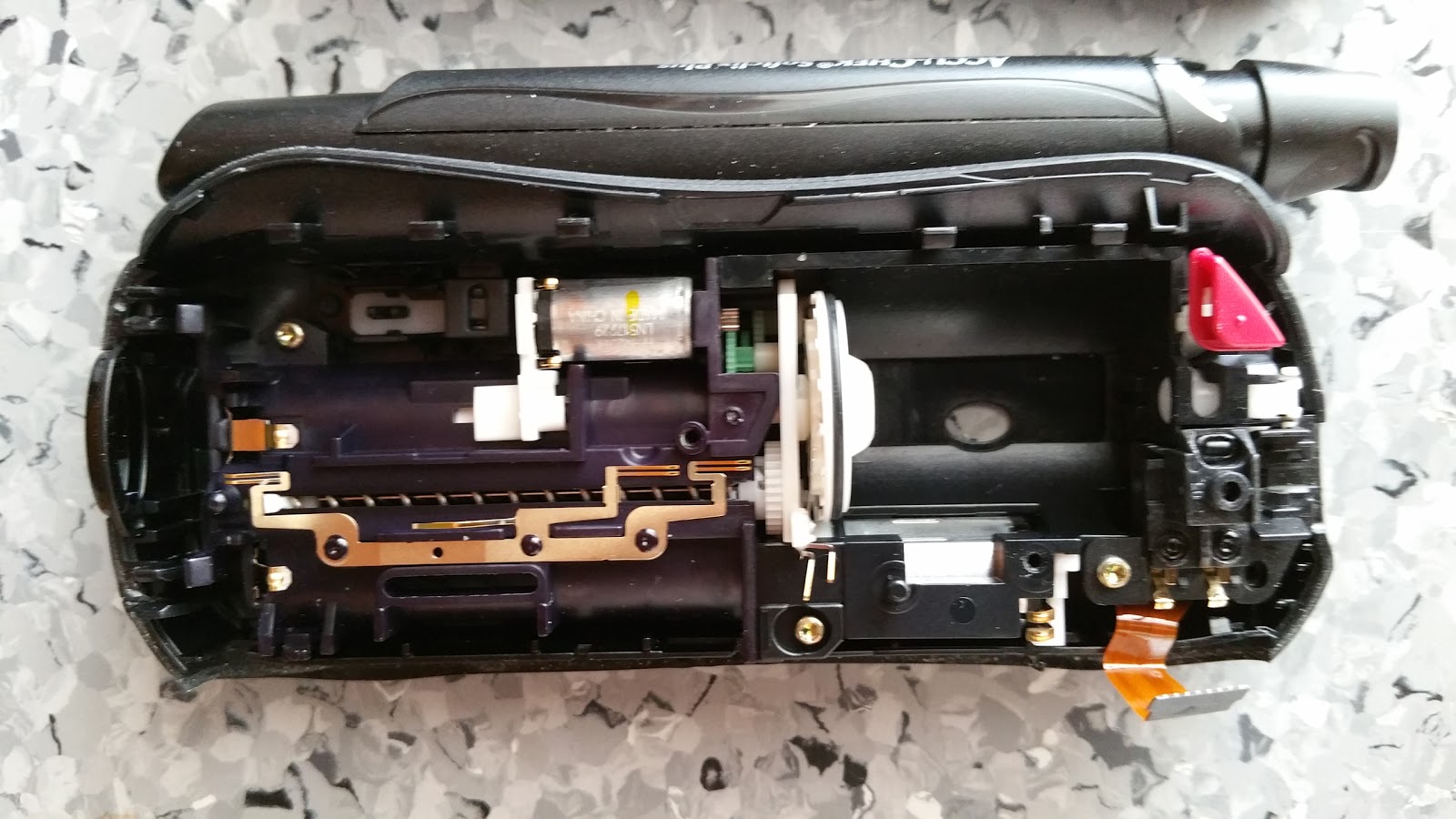
At first, doesn't seem like much, but things are really nice and compact inside. This is how it looks with the front off. The cavity on the right (Marked with blue) is where the drum of test strips goes in.
A motorized rod (Marked with red) pushes a strip out of  the drum and through the glucose sensor (Marked with purple)


Now, to detect glucose in the blood, there are two main ways. 
One is electrochemical in nature. You get the glucose in the blood to react to an agent on the test strip. Electrodes on the strip allow a bias voltage to be fed through and then  the current is measured, which is proportional to the amount of glucose in the blood. The full scale current would be somewhere around  10-50 µA (http://www.maximintegrated.com/en/app-notes/index.mvp/id/4659)

The other way to do it is by optical measurement. When a blood sample is placed on the test strip, this will change color according to the glucose concentration. A LED diode biased with a known current is shone onto the test strip and a photo-diode senses the reflected light, who's intensity is dependent on the color of the strip. From what I've read, the biasing current is somewhere from 1µA to 5µA. This is the method also used in the Accu-Check Compact.


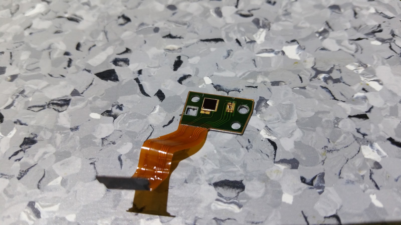
This is a close-up of the sensor. I've marked the window for the LED and photo-diode.


And this is the actual array, with the LED on the right and the photo-diode on the left.

And not, let's see how the PCB for this thing looks like.


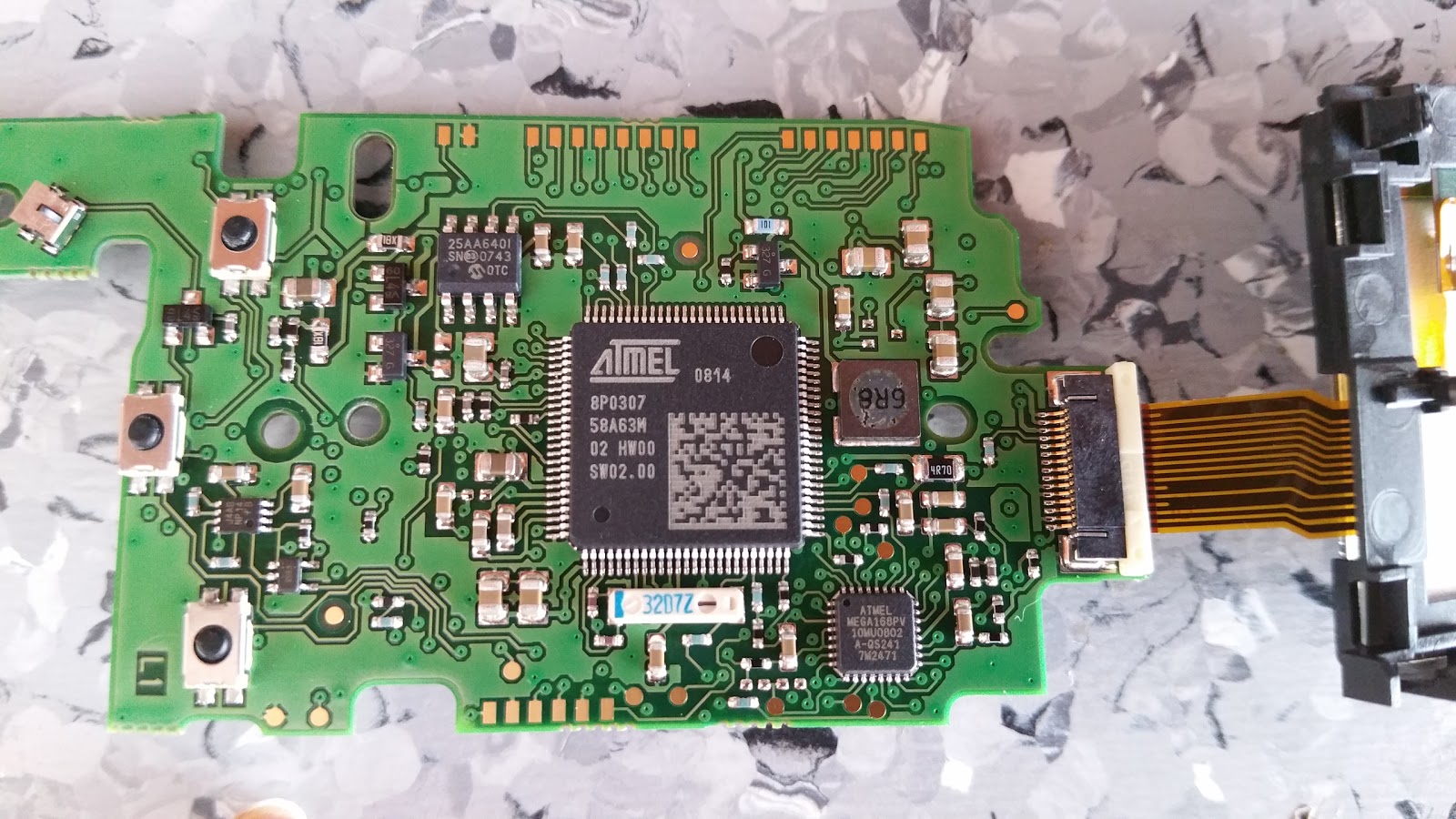
Looks well made and designed. On the right, you can see the OLED display this thing uses. It's based on the SSD1325 controller, for those that are wondering, so it should be relatively easy to take this out and use it for something else. The big black square on the PCB is actually a piezo-transducer, (Datasheet here) for whatever sounds this thing makes.
A nice thing to notice are the multitude of test pads on the board. Being a medical device, probably there's a lot of things that need to be spot on for it to pass whatever standards that concern this specific field. Also, probably there's a bit of calibration going into this meter.

There's also an infrared comm. port on this thing, probably for downloading all the history data onto a PC or something like that. Haven't tried playing with that, so I can't tell for sure, but from the manufacturer's data, that might indeed be the  case.

Also, after some searches, I found out that someone else took apart one of these glucose meters and hacked the display, which I'm going to do pretty soon. Information on that can be found here: http://home.arcor.de/wehrsdorf/Oled-Display-Recycling.html

There's also a bit of grunt built into this meter, when it comes to processing power.


That's most likely  an ARM processor from Atmel, for the doing all the math and driving the infrared port and motors and whatever else on the board  needs some  smarts behind it. For the actual OLED display, there's an ATMEL Mega 168 micro, which I will soon acquaint myself with, in order to get the display going.

What I was  really curious about was  the  ADC that reads the photo-diode and also driver for the LED diode. From what I read, there must be some really precise measurements done in order to get accurate  readings.


Link to Picasa Teardown Album

Wednesday, July 22, 2015

What's this page about? Also first book recommendation

Maybe some of you are wondering what's this doing here? What's up with this?

Well, in this section, I'll be posting  reference design books, service and user manuals for test gear that I own, schematics and so on, both to create a library of data for myself and also to maybe help others that are searching for ideas, manuals....

So, let me start this off with a recommendation for those that are just starting with electronics and also for those that have the experience but never managed to read this book:

"The Art of Electronics" by Paul Horowitz and Winfield Hill - Second Edition

This is the go-to book if you're a student and also if you have some experience but having trouble with either understanding something or struggling with a design.
This edition is indeed old (1987-1988 I think) but most of it holds true even today, especially  for the analog and linear chapters.

I will not be making a review of this book because there are way too many out there. Having read it myself, I think it is essential that every electronics engineer try to go through this so one can gain a basic understanding of all things electronics. It is by no means complete, and again, it is very old, but hey, it's cheaper that the Third Edition (if you know where to download it from wink! wink!) and it'll keep you busy for quite a while.

So, have fun reading, or just stay on this blog for a while longer and enjoy the eye candy.

HP 3478A Multimeter Power Button Fix

   In the post about the HP 3478A Multimeter Modification, I said at one point that even though there's that issue about the stuck power switch, it doesn't bother me that much.
Well, it turns out that it did bother me. In fact it was down right annoying. Most likely because of my O.C.D. was acting up, knowing that there's something not quite right about the multimeter.

So, rummaging through my collection of old miscellaneous "things" I salvaged from different other devices people usually throw away (yes good people, sometimes,  being a hoarder really pays off), I happened to find a spring power switch, which, in mind mind looked like a very good replacement for the one on the HP multimeter.

So, I quickly took the top cover off my 3478A, had a quick peek at the broken power button, and indeed, looked very much like the one I recently found. So, I naturally thought "well, OK, I'll replace it now....how hard cand it be....should't take more than half an hour, right?" Famous last words.

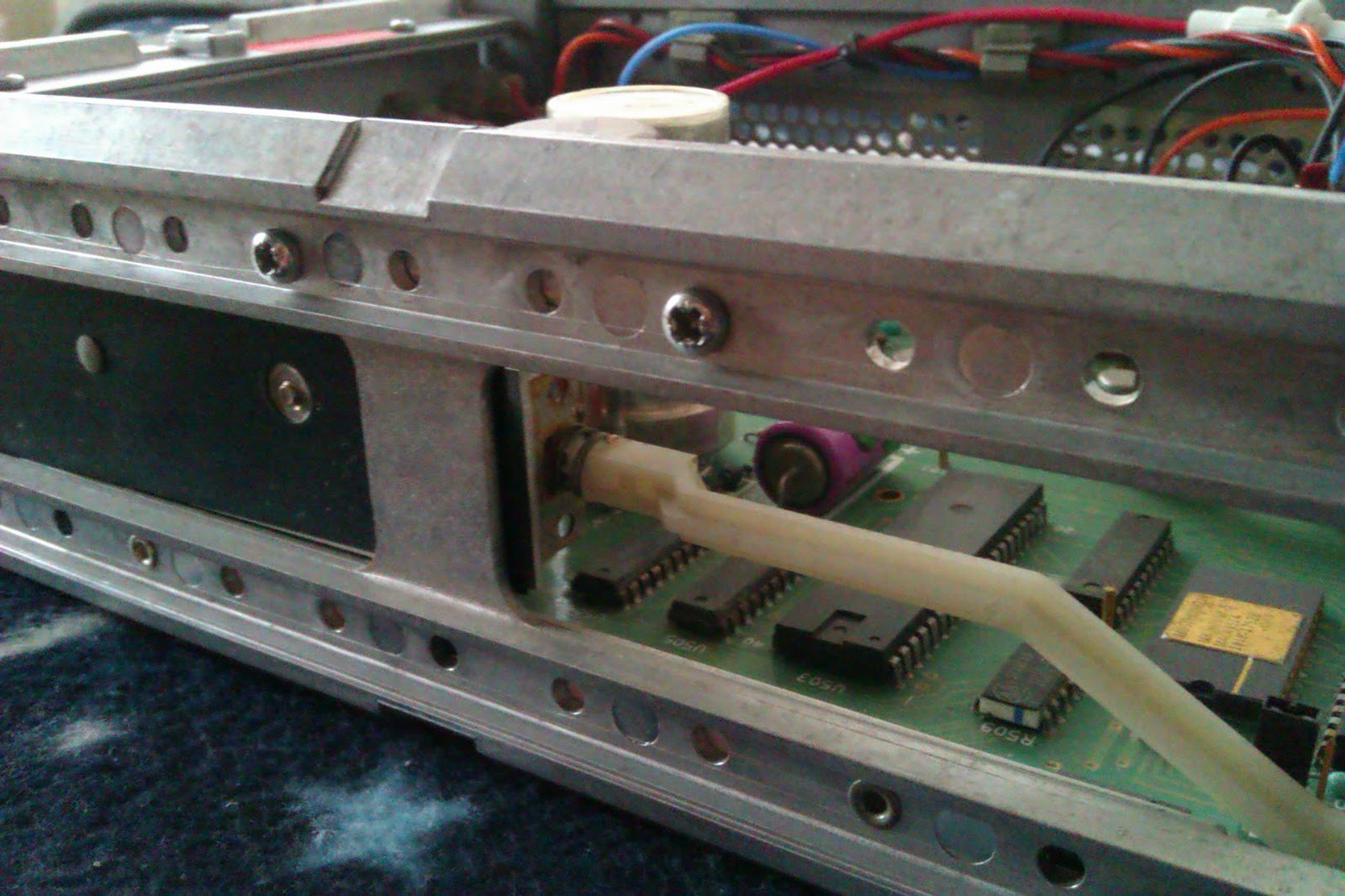
Took me a few minutes to figure out just how to take apart the 3478A to get to the power button. First, the side plate had to be removed, exposing the cast aluminium frame.


So, ignoring the very fashionable bed  covers (that's how real engineers work....on beds and chairs  and garages) the frame is held in place with four screws, one in each corner. Screwed to this frame piece is an aluminium plate that holds the transformer, a voltage regulator and also the infamous power switch.

After first unscrewing the  three bolts that hold the aluminium plate, I then undid the four corner screws and took off the frame piece.


Nope, still not there just yet. The screws that hold the power button are now accessible, but to get the whole power button out, the plate also has to come off. For this, the two screws that hold the transformer to the plate need to be  taken out also. Only after this, can the aluminium plate be lifted, thus giving access to the button.


If undertaking something of this sorts, take care how you handle the wires going to the regulator. Careful the solder doesn't crack or that you don't put too much stress on the wires themselves, because they might sometimes crack because of old age (although mine looked pretty good, despite the unit being  built in 1991).

OK, pretty good so far. Now what?  Well, take out the button, right? Out with the old, in with the new..er.
I took my trusty needle nose pliers, grabbed the shaft of the button and pulled it apart from the lever of the button than protrudes out from the front panel.
The, with a scalpel, I cut the shrink tube from around the power button and lo and behold...two capacitors and two resistors on the sides of the button...man, the guys at HP weren't stingy at all. Very nice bit of kit they built here. Annoying as hell because now I had to do even more work on it, but  nice attention to detail.


This is the part where I started to take the replacement button and measuring it up along side the original and see if it really fits....Well, not really. The shaft of the replacement is about 5 millimeters longer and  it also had a much wider metal plate on the front.


In the picture above you can see the solution. I took the metal bezel (front plate, call it what you will) from the original HP button and stuck it onto this. I don't know if it was divine intervention or just pure dumb luck, but somehow, I only has to file away about 1 millimeter so that the plate could snugly fit onto the new button. Also, in the picture above, you can see the original plate on the right, and the old plate already installed on the new button (new-ish, anyway).
The next steps may sound straight forward, but it took me about 30 minutes to do. After filing away the shaft so it would fit into the lever and then cutting the lever about 5 millimeters and also the shaft of the button another 5 millimeters, I took off (no, not desoldered, but "took off", as in "cut off") the capacitors and resistors from the old switch and soldered them to the replacement one.
The original HP switch was a  Schadow,  Type NE15, DPDT switch. The replacement was a  DPST one, but that worked, since HP also used it in this configuration.

A quick mockup seemed promising as the button and the lever seemed to fit and more importantly, actually worked.

By the way, I didn't have shrink  tube that large a diameter, so I put some electrical tape around the button to insulate it. May sound crude, may look even cruder, but it works and is also a very viable long term solution.


It may sound simple, all of this, but the whole taking the plate apart, figuring how to make the replacement button fit then soldering the wires and components to it, putting it back together, took a little over two hours.

So, fun as it was, this is  one of those things that you'd only do once. But at least, in the end, I now have a fully functioning multimeter.


Tuesday, July 14, 2015

HP 3478A Multimeter Modifications

    What kind of electronics engineer doesn't have a bench multimeter? Well, probably a lot, but since I didn't have any decent multimeter, aside from some very cheap UNI-T ones, I bought from eBay an old HP 3478A 5 1/2 digit multimeter.
It'd old, I know, but it was "really cheap" (about 120 Euros) and only had some minor faults. I mean, what's a stuck Power button and a missing AMPs range fuse, right?


So, anyhow, it arrived, I was thrilled when I got it and surprise surprise, it worked surprisingly well and gave very accurate readings (tested it against another, borrowed, Fluke  handheld multimeter and it was very accurate).

And, now what?  Well, the Power button was stuck in the "On" position, which is very convenient, so for now, until I can get a replacement switch, I'll just have to unplug it when its job is done. (the button is  all rusty and full of crud)

I proceeded to put it through its paces and measured....stuff.  I asked someone to lend me a Fluke DMM. Then, the rest was simple. For the  DC volts, a home made, dual channel power supply,  with 0-30 Volts on each channel proved very helpful and also a variable transformer for the AC volts helped, although, kind of tricky because the line voltage isn't really an ideal standard because of the constantly changing loading of the grid. The 2-wire and 4-wire Ohms also worked a treat.

As for the missing AMPS fuse....This thing has plugs in the back also, right? Which I'm not going to use, right? So, why not disconnect the wire from the front AMPS plug, run a fuse and a wire to some other pug to the rear terminals and that's it. So I did just that. I ordered a fuse-holder and some 3A 250V fast fuses, cut the original Amps range wire,  spliced it with the fuse holder and Voila! A fully functioning bench multimeter.


Also, if someone's curious, yes, I checked the battery for the ROM that holds the calibration data and it was either changed or still has some life in it, because it read about 3.6 Volts.

Future thoughts  - get a GPIB PCI card and start putting this little jewel to some good use in some automated tests for one of my projects I've been working on lately.

Teardown of an old russian C1-91 100 MHz, 2 Channel Oscilloscope


 I got this old relic for free from a very kind person, when I was still a student and working on my final year project. It's a great bit of kit, and, yes, it's a clone of the Tektronix modular scopes from the 80's, and yes, the labels are all in Russian, and yes, it takes 10 minutes for the CRT to actually show something....but hey, it did it's job. 
But now, since I  got my new Rigol 1054Z and because the trigger on the old C1-91 has been trowing fits, I figured that it was just taking up space. Plus I just couldn't find a spot in a corner somewhere where it could sit undisturbed and hot have to move it every time I cleaned my room / lab, because this thing is heavy....about 30 kilograms worth. So I decided I could do without it and maybe use the components inside for other things, like an oscilloscope clock for example.

So, taking after it's clone, the Tektronix 7000 series Mainframe oscilloscopes, it has three bays where one can mount different modules, from a two channel oscilloscope input module, to a multimeter module, signal generator modules and so on. I removed mine, then proceeded to disassemble it to it's bare bones. Easier said that done, and I'll explain why.
The people that designed this scope were either thinking, or blindly copied every detail from the Tektronix scopes. I, personally, since I haven't seen the insides of said Tektronox scopes, would like to believe the first option, that the russian  engineers knew what they were doing.
Because the frame of the scope was all aluminium, it only makes sense that to avoid corrosion pr oxidation, same metal fastners have to be used. Therefore, all the screws on the aluminium parts were also made of aluminium. Which would be nice, if they weren't made from the softest alloy they could find. And when I say soft, I mean that by applying a bit of force  to loosen the Phillips head screws was enough to mangle them and so, be stuck in place.
Oh well....where there's a hammer, there's a way.

The first thing one notices when taking such  devices apart is how different they look. Back then, the Russians made their own electronic components (capacitors, resistors, diodes, transistors of all kinds, ICs), after their own liking and in the process, developed a style of their own, to laying out boards.


See what I mean. By the way, the square metal cans are actually hybrid circuits.
Trust me when I say it's weird. And don't even get me started on the schematic. In fact, as I'm  writing this, I'm trying to figure out the schematics for this thing, so that I can turn it into  a prototype for an oscilloscope clock and sincerely, not getting anywhere with it. I mean, they have all kinds of numbered wires going all over the place to numbered connectors. But the same wire has different markings on each end and each pair of connectors (from one board to another) also have different names, making things very frustrating and hard to read. A post with my efforts on the scope clock will follow at some point.

Until then, I leave you with the Picasa album with teardown pictures for this thing so you can admire this in its full glory and actually get a feel for how bulky this thing is and feels.


Thursday, July 2, 2015

Teardown of old NEC MultiSync MT Projector

        A few months ago I got my hands on an old NEC Projector from the local flea market for almost nothing (20 Euros or so).
Of course, after carrying up the stairs to my apartment, which is no mean feat, because this thing weighs about 30 kilos, I followed the normal procedure for such a nice piece of old "vintage" electronic gear, which was to stand back and admire it. Ain't she a beaty?


 After getting my trusty screwdriver set out, first I wanted to see the lamp in this thing. Pretty ordinary for it's day, but what really surprised me was that it probably had been recently replaced - or so it said in the menu. Only 600 hours of run-time? What a score.

So why take apart a perfectly functional projector? Well, for one, the 640x480 maximum resolution this thing has isn't really of much use....for anything. Another reason is that it has lots of nice components which are worth much more than what I pain for it. But the main reason is curiosity. I just want to rip it open then drool over it while I try and figure out what everything does.

So,  first thing, the lamp. Looks nice an beefy, and really nice thing that the High Voltage power supply for this works independently of the projector's "mother board". Of course I couldn't resist not playing with it.


Top notch job on this. Looks like the engineers that worked on this design did a really nice job. I mean, it did cost about 10.000 dollars new....back in the 90's.
In fact, this entire thing was really nicely engineered and  with quality parts. Rubycon and Nichicon caps, Omron relays, really nice BNCs and connectors on the front. And also, a ton of quality optics in it.


                                                   (FYI:That's in centimeters, not inches)


After making my way through the jungle of wires inside this thing, I finally got to the main power board. As I said, really nice design. No cheap Wan-Hung-Lo brand caps here, thank you very much.
Input filter, MOVs, this thing's got it all.
The board is mainly dedicated to the switch-mope supply, but there's also a smaller transformer, probably powering the analog part of the main logic board i.e the op-amps for the video output.
Also, notice the amount of EMI suppression this board has on it (especially the analog section), and also  the forest of electrolytics scattered all over.

It took me the better part of a day to get to the metal chassis for the optics  of the projector. Everything was either  tied down with cable ties  or screwed to something. Like I said...quality.
But once I got to the optics....


I spent another day carefully getting every mirror out and the trying to figure out how this thing actually produced an image.
And this is what I came up with:


Excuse the hand drawn schematic, but I really suck when it comes to expressing my inner artist.
Basically, the light from the lamp is split into three optical pathways, each corresponding to the colors  Cyan, Magenta and Yellow. This is done with two dichroic mirrors. For those that don't know what a dichroic mirror is (don't worry, I didn't  know either before this teardown), it's a mirror that only reflects a certain wavelength of light, while letting the rest of the spectrum to freely pass through it without much disturbance (i.e. reflections or refractions).
There are also two other "normal" mirrors that are there only to help guide the light to the  main  objective.
Now, after the colors have been separated, the image has to be produced somehow. This is where three LCD displays come in. The video data is taken from the input panel,  then the processor  splits that up into three colors, then sends each color channel data to the LCDs. The LCDs are almost transparent (they have a darkish tinge to them) so some  light is lost at this stage. Also, in front of two of the LCDs there are polarizing filters - one vertical and the other horizontal. I haven't quite figured this part out yet, I don't know how they tie up in the final image.
From here on, all that;s left to do is join the three optical path with some clever use of optics into one beam, then send it on it's way to be projected on to whatever surface  someone desires (as long as it's white).

Now, I'd like to mention that although it's much nicer for the eye to have this kind of splitting of the video data into three separate  colors, it's expensive as you need a lot of quality optics. Also there is a lot of light lost because the dichroic mirrors do not reflect 100% of the light and because the LCDs are somewhat dark, so the final image looks really dim. So a lot of light is needed to be pumped into this thing to get  a relatively ok picture on the other end.
So, that's why we're stuck with the color wheel in today's projectors that make you see stars every time you rapidly move your eyes when looking at a modern projector (or should I say the image projected by it)

If you would like to know more about the color wheel I mentioned, watch this video that Ben Krasnow made, detailing how modern projectors work. It's worth it, trust me.

For more information on this projector, you can visit: http://www.projectorcentral.com/NEC-MultiSync_MT.htm


google-site-verification: googlee8a41f51abde7545.html