I know there's a ton of blogs and articles on the matter of DIY PCB making, and for every hundred articles, there's a hundred different ways to do it.
So here, I'll just present you the way I do my PCBs. It's pretty simple and cost effective, not to mention I get good results...most of the time.
Things needed:
- A4 Laminator (I use a Peach PL718)
- Glossy A4 paper (150 gramms)
- Ferric chloride
- A large glass bowl
- An even larger plastic dish (for hot water)
- Isopropanol alcohool
- Plastic gloves
- 800 grit sandpaper (if needed)
- Laser Printer
And now, how I use the above mentioned items. Well, first, it's important to have a flat laminator. Meaning that the paper, or in this case the PCB should go in and come out flat and not at an angle, because, for obvious reasons, the fiberglass material isn't all too "bendy".
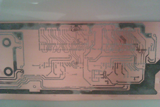
 This is a recent board I did. It's about 300 mm in length, so heat dissipation can become an issue.

The paper I use is glossy 150 grams A4 paper. It can be of higher weight, maybe up to 250 grams, but the most important thing here is that the paper must be glossy. That will allow for all the toner to stick to the PCB and give you a nice solid transfer, that will not flake off when you remove the paper. Regular A4 paper just won't do. I've tried it, and the result is crap. The toner transferred to the PCB will be easily rubbed off with your fingers, if you use the regular paper.
So, needless to say, the next step is to use you PCB software to make your board design, the you print it out on a laser printer, on the mentioned type of paper. The type of toner is somewhat important, but most will give you a very decent result. Just do not forget to set your printer to print o heavy paper. This will have the effect of depositing a thicker amount of toner, which is exactly what you need.


If the PCB has been lying around for a long time, in open air, it might have an oxide layer on it that will prevent the toner adhering. So I take some 800 grit sandpaper and give the copper a gentle rub. If you don't have any lying around, you could use some steel wool.
Then, wash the board under a stream of water then with some tissues soaked in isopropanol, give it another cleaning to get rid of the fine dust.
Then, wash the board under a stream of water then with some tissues soaked in isopropanol, give it another cleaning to get rid of the fine dust.
Next is setting things up for the toner transfer. As a common practice, I stick the paper to the PCB with a little Kapton tape so it doesn't wonder off when it goes through the laminator. I don't recommend using scotch tape or masking tape because the scotch tape will melt and ruin your day and the masking tape is too thick and any toner that is under that area will not be pressed down by the rollers of the laminator. Also, make sure the Kapton tape is in an area where there is no toner underneath, because of the same reason I mentioned for the masking tape.
I make about 10 to 20 passes on the laminator, depending on the board size and level of details of the tracks (spacing and track width). I basically just go with my gut instinct, but a rule of thumb for me, is after the board gets up to temperature (the temperature where I need a glove to handle the board), I do about 6 or 7 more passes, then that's it.
After it's cooled for a bit, I put the PCB with the stuck-on paper in some warm water and let it sit for 5 minutes. Then I peel most the paper off and the rest rub it off with my fingers or use a toothbrush. If the toner or the paper are not OK, this is where it shows. If you use the toothbrush, or just you fingers, no toner should flake off, even if you give it a firm rub. If it does, then either try another type of (glossy) paper or try with another laser printer.


All you need to do now is etch away the copper. I use a "bain Marie" for this part. I put the ferric chloride in a glass bowl (this should be large enough to accommodate the PCB but not too large, because it will cause you to use too much etchant) and then I place this in a larger plastic dish full of hot water. Warm ferric chloride will work much faster than if you leave it at room temperature.
Also, if you leave it to just sit, it will take a fairly long time for the whole copper to etch away, that's why I hold the glass bows in the water and constantly move it side to side (the idea is to keep the liquid moving in the glass dish).
In about 10 minutes, a 5cm x 5cm board should be ready. Don't forget to wear some plastic or latex gloves, because the etchant stains. And do this in a ventilated place, as the process will release Chlorine fumes. And Yes!, Chlorine is bad for you! - that's why they put it in water, to kill every living thing in there.
In about 10 minutes, a 5cm x 5cm board should be ready. Don't forget to wear some plastic or latex gloves, because the etchant stains. And do this in a ventilated place, as the process will release Chlorine fumes. And Yes!, Chlorine is bad for you! - that's why they put it in water, to kill every living thing in there.
After you can't see any more copper except the one covered by the toner, remove the board, wash the etchant off under a stream of water (again, careful here, because the ferric chloride stains you skin and anything else it touches ).
After you admire you masterpiece and brag to anyone in the house at that moment, use a stainless steel sponge or steel wool to remove the toner off the copper. Again, do this under a stream of warm water.
At the end you should be left with a nice, fresh PCB, ready for tinning and drilling some holes (if it's for Through-hole). I've tried this method for track widths down to 0.4 mm and it works great. You could push it down to 0.3 without any issue, but that depends on your luck and skill. Too much temperature and too much pressure may cause the narrower tracks to flatten out and actually get wider.
Again, this is how I do things. It's worked so far, even for some SMD boards, but if you design a board with really fine pin pitch, I'd recommend the UV exposure method.
It's OK if things don;t work out first go. As you can see below:
This is an example why the printer and toner a very important. Here, the printer did not deposit enough toner on the paper, even though the settings were for heavy paper. So it's all about experimenting, to find the right printer that works for you, or the right settings on a printer you already have.
This is the second go, and the result is much better:
It's OK if things don;t work out first go. As you can see below:

This is an example why the printer and toner a very important. Here, the printer did not deposit enough toner on the paper, even though the settings were for heavy paper. So it's all about experimenting, to find the right printer that works for you, or the right settings on a printer you already have.
This is the second go, and the result is much better:

So the conclusion is, experiment, find what works for you, then stick with it.
Also, you might find that for through-hole boards that have thick traces, one process might apply, but for SMD boards, you might go with a UV exposure method maybe.


